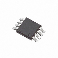
ZXMD63N03XTC Diodes Zetex, ZXMD63N03XTC Datasheet - Page 2

ZXMD63N03XTC
Manufacturer Part Number
ZXMD63N03XTC
Description
MOSFET DUAL N-CHAN 30V 8MSOP
Manufacturer
Diodes Zetex
Datasheet
1.ZXMD63N03XTA.pdf
(7 pages)
Specifications of ZXMD63N03XTC
Fet Type
2 N-Channel (Dual)
Fet Feature
Logic Level Gate
Rds On (max) @ Id, Vgs
135 mOhm @ 1.7A, 10V
Drain To Source Voltage (vdss)
30V
Current - Continuous Drain (id) @ 25° C
2.3A
Vgs(th) (max) @ Id
1V @ 250µA
Gate Charge (qg) @ Vgs
8nC @ 10V
Input Capacitance (ciss) @ Vds
290pF @ 25V
Power - Max
870mW
Mounting Type
Surface Mount
Package / Case
8-MSOP, Micro8™, 8-uMAX, 8-uSOP,
Lead Free Status / RoHS Status
Lead free / RoHS Compliant
ABSOLUTE MAXIMUM RATINGS
THERMAL RESISTANCE
NOTES:
(a) For a device surface mounted on 25mm x 25mm FR4 PCB with high coverage of single sided 1oz copper, in still air conditions
(b) For a device surface mounted on FR4 PCB measured at t 10 secs.
(c) Repetitive rating - pulse width limited by maximum junction temperature. Refer to Transient Thermal Impedance graph.
(d) For device with one active die.
(e) For device with two active die running at equal power.
ISSUE 1 - OCTOBER 2005
PARAMETER
Drain-Source Voltage
Gate- Source Voltage
Continuous Drain Current
Pulsed Drain Current (c)(d)
Continuous Source Current (Body Diode)(b)(d)
Power Dissipation at T
Linear Derating Factor
Power Dissipation at T
Linear Derating Factor
Power Dissipation at T
Linear Derating Factor
Operating and Storage Temperature Range
PARAMETER
Junction to Ambient (a)(d)
Junction to Ambient (b)(d)
Junction to Ambient (a)(e)
Pulsed Source Current (Body Diode)(c)(d)
A
A
A
=25°C (a)(d)
=25°C (a)(e)
=25°C (b)(d)
(V
(V
GS
GS
=4.5V; T
=4.5V; T
A
A
=25°C)(b)(d)
=70°C)(b)(d)
SYMBOL
R
R
R
2
θJA
θJA
θJA
SYMBOL
V
V
I
I
I
I
P
P
P
T
D
DM
S
SM
D
D
D
j
DSS
GS
:T
stg
-55 to +150
VALUE
143
100
120
LIMIT
0.87
1.04
1.25
±20
2.3
1.8
1.5
6.9
8.3
ZXMD63N03X
30
14
14
10
S E M I C O N D U C T O R S
mW/°C
mW/°C
mW/°C
UNIT
°C/W
°C/W
°C/W
UNIT
°C
W
W
W
A
A
A
A
V
V


