SI7501DN-T1-GE3 Vishay, SI7501DN-T1-GE3 Datasheet - Page 7
SI7501DN-T1-GE3
Manufacturer Part Number
SI7501DN-T1-GE3
Description
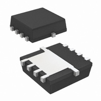
MOSFET N/P-CH 30V PPAK 1212-8
Manufacturer
Vishay
Datasheet
1.SI7501DN-T1-GE3.pdf
(9 pages)
Specifications of SI7501DN-T1-GE3
Package / Case
PowerPAK® 1212-8
Fet Type
N and P-Channel
Fet Feature
Logic Level Gate
Rds On (max) @ Id, Vgs
35 mOhm @ 7.7A, 10V
Drain To Source Voltage (vdss)
30V
Current - Continuous Drain (id) @ 25° C
5.4A, 4.5A
Vgs(th) (max) @ Id
3V @ 250µA
Gate Charge (qg) @ Vgs
14nC @ 10V
Power - Max
1.6W
Mounting Type
Surface Mount
Transistor Polarity
N And P Channel
Drain Source Voltage Vds
30V
Power Dissipation Pd
1.6W
Operating Temperature Range
-55°C To +150°C
Termination Type
SMD
Filter Terminals
SMD
Rohs Compliant
Yes
Lead Free Status / RoHS Status
Lead free / RoHS Compliant
Other names
SI7501DN-T1-GE3TR
Available stocks
Company
Part Number
Manufacturer
Quantity
Price

Part Number:
SI7501DN-T1-GE3
Manufacturer:
VISHAY/威世
Quantity:
20 000


N-CHANNEL TYPICAL CHARACTERISTICS 25 °C, unless otherwise noted
Document Number: 72173
S-81544-Rev. D, 07-Jul-08
- 0.2
- 0.4
- 0.6
- 0.8
0.4
0.2
0.0
30
10
1
- 50
0.0
- 25
Source-Drain Diode Forward Voltage
0.2
V
SD
0
0.4
- Source-to-Drain Voltage (V)
Threshold Voltage
T
J
T
25
- Temperature (°C)
J
= 150 °C
0.6
I
D
50
= 250 µA
0.8
75
1.0
0.01
100
100
0.1
10
T
1
J
0.1
= 25 °C
* V
1.2
125
Limited by R
Limited
GS
I
Single Pulse
D(on)
T
> minimum V
A
150
1.4
= 25 °C
V
DS
Safe Operating Area
DS(on)
- Drain-to-Source Voltage (V)
1
GS
*
at which R
BV
DSS
Limited
DS(on)
0.16
0.12
0.08
0.04
0.00
10
50
40
30
20
10
0
10
0
I
is specified
DM
- 3
On-Resistance vs. Gate-to-Source Voltage
Limited
P(t) = 0.0001
P(t) = 0.001
P(t) = 0.01
P(t) = 0.1
P(t) = 1
P(t) = 10
DC
10
2
-2
100
V
GS
Single Pulse Power
- Gate-to-Source Voltage (V)
10
-1
4
I
D
Time (s)
= 7.7 A
Vishay Siliconix
1
6
Si7501DN
10
www.vishay.com
8
100
600
10
7
Related parts for SI7501DN-T1-GE3
Image
Part Number
Description
Manufacturer
Datasheet
Request
R

Part Number:
Description:
MOSFET N/P-CH 30V PWRPAK 1212-8
Manufacturer:
Vishay
Datasheet:

Part Number:
Description:
Complementary 30-V (D-S) MOSFET
Manufacturer:
Vishay Intertechnology
Datasheet:

Part Number:
Description:
Complementary 30-v D-s Mosfet
Manufacturer:
Vishay
Datasheet:
Part Number:
Description:
357-036-542-201 CARDEDGE 36POS DL .156 BLK LOPRO
Manufacturer:
Vishay
Datasheet:
Part Number:
Description:
357-036-542-201 CARDEDGE 36POS DL .156 BLK LOPRO
Manufacturer:
Vishay
Datasheet:
Part Number:
Description:
357-036-542-201 CARDEDGE 36POS DL .156 BLK LOPRO
Manufacturer:
Vishay
Datasheet:
Part Number:
Description:
357-036-542-201 CARDEDGE 36POS DL .156 BLK LOPRO
Manufacturer:
Vishay
Datasheet:
Part Number:
Description:
357-036-542-201 CARDEDGE 36POS DL .156 BLK LOPRO
Manufacturer:
Vishay
Datasheet:
Part Number:
Description:
357-036-542-201 CARDEDGE 36POS DL .156 BLK LOPRO
Manufacturer:
Vishay
Datasheet:
Part Number:
Description:
357-036-542-201 CARDEDGE 36POS DL .156 BLK LOPRO
Manufacturer:
Vishay
Datasheet:
Part Number:
Description:
357-036-542-201 CARDEDGE 36POS DL .156 BLK LOPRO
Manufacturer:
Vishay
Datasheet:
Part Number:
Description:
357-036-542-201 CARDEDGE 36POS DL .156 BLK LOPRO
Manufacturer:
Vishay
Datasheet:
Part Number:
Description:
357-036-542-201 CARDEDGE 36POS DL .156 BLK LOPRO
Manufacturer:
Vishay
Datasheet:
Part Number:
Description:
357-036-542-201 CARDEDGE 36POS DL .156 BLK LOPRO
Manufacturer:
Vishay
Datasheet:
Part Number:
Description:
357-036-542-201 CARDEDGE 36POS DL .156 BLK LOPRO
Manufacturer:
Vishay
Datasheet: