NTHD4508NT1G ON Semiconductor, NTHD4508NT1G Datasheet
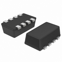
MOSFET 2N-CH 20V 3.1A CHIPFET

NTHD4508NT1G

Manufacturer Part Number
NTHD4508NT1G
Description
MOSFET 2N-CH 20V 3.1A CHIPFET
Manufacturer
ON Semiconductor
Datasheet

Specifications of NTHD4508NT1G

Fet Type
2 N-Channel (Dual)
Fet Feature
Logic Level Gate
Rds On (max) @ Id, Vgs
75 mOhm @ 3.1A, 4.5V
Drain To Source Voltage (vdss)
20V
Current - Continuous Drain (id) @ 25° C
3A
Vgs(th) (max) @ Id
1.2V @ 250µA
Gate Charge (qg) @ Vgs
4nC @ 4.5V
Input Capacitance (ciss) @ Vds
180pF @ 10V
Power - Max
1.13W
Mounting Type
Surface Mount
Package / Case
8-ChipFET™
Configuration
Dual Dual Drain
Transistor Polarity
N-Channel
Resistance Drain-source Rds (on)
0.075 Ohm @ 4.5 V
Forward Transconductance Gfs (max / Min)
6 S
Drain-source Breakdown Voltage
20 V
Gate-source Breakdown Voltage
+/- 12 V
Continuous Drain Current
3 A
Power Dissipation
1130 mW
Maximum Operating Temperature
+ 150 C
Mounting Style
SMD/SMT
Minimum Operating Temperature
- 55 C
Lead Free Status / RoHS Status
Lead free / RoHS Compliant
Other names
NTHD4508NT1GOSTR

Available stocks

Company
Part Number
Manufacturer
Quantity
Price
Part Number:
NTHD4508NT1G
Manufacturer:
ON Semiconductor
Quantity:
35 997
Part Number:
NTHD4508NT1G
Manufacturer:
ON/安森美
Quantity:
20 000
NTHD4508N
Power MOSFET
20 V, 4.1 A, Dual N−Channel ChipFETt
Features
Applications
Maximum ratings are those values beyond which device damage can occur.
Maximum ratings applied to the device are individual stress limit values (not
normal operating conditions) and are not valid simultaneously. If these limits are
exceeded, device functional operation is not implied, damage may occur and
reliability may be affected.
1. Surface Mounted on FR4 Board using 1 in sq pad size (Cu area = 1.27 in sq
October, 2004 − Rev. 3
MAXIMUM RATINGS
THERMAL RESISTANCE RATINGS
Drain−to−Source Voltage
Gate−to−Source Voltage
Continuous Drain
Current
Current
Power Dissipation
Pulsed Drain Current
Operating Junction and Storage Temperature
Lead Temperature for Soldering Purposes
(1/8” from case for 10 s)
Junction−to−Ambient – Steady State
(Note 1)
Players, Cell Phones, DSCs and PDAs
Low R
Leadless ChipFET Package has 40% Smaller Footprint than TSOP−6
Excellent Thermal Capabilities Where Heat Transfer is Required
Pb−Free Package is Available
DC−DC Buck/Boost Converters
Battery and Low Side Switching in Portable Equipment Such as MP3
Level Shifting
Semiconductor Components Industries, LLC, 2004
[1 oz] including traces).
DS(on)
Parameter
and Fast Switching Speed
Parameter
(T
Steady
Steady
t v 5 s
Steady
Steady
t v 5 s
State
State
J
= 25 C unless otherwise noted)
t
p
= 10 s
T
T
T
T
T
T
J
J
J
J
J
J
= 25 C
= 85 C
= 25 C
= 25 C
= 85 C
= 25 C
Symbol
R
Symbol
JA
V
T
V
I
P
T
DSS
DM
STG
T
I
GS
D
J
D
L
,
Max
110
−55 to
Value
1.13
0.59
150
260
3.0
2.2
4.1
2.1
20
12
12
1
Unit
Unit
C/W
W
V
V
A
A
C
C
†For information on tape and reel specifications,
NTHD4508NT1
NTHD4508NT1G
including part orientation and tape sizes, please
refer to our Tape and Reel Packaging Specification
Brochure, BRD8011/D.
D
D
D
D
V
CONNECTIONS
1
1
2
2
(BR)DSS
20 V
Device
8
7
6
5
G
ORDERING INFORMATION
1
PIN
, G
C8 = Specific Device Code
M = Month Code
2
http://onsemi.com
N−Channel MOSFET
1
2
3
4
60 mW @ 4.5 V
80 mW @ 2.5 V
R
(Pb−Free)
Package
D
ChipFET
ChipFET
S
G
S
G
DS(on)
1
1
2
1
2
, D
Publication Order Number:
2
TYP
1
2
3
4
CASE 1206A
S
MARKING
DIAGRAM
1
ChipFET
STYLE 2
3000/Tape & Reel
3000/Tape & Reel
, S
2
Shipping
NTHD4508N/D
I
D
4.1 A
MAX
8
7
6
5

Related parts for NTHD4508NT1G

NTHD4508NT1G Summary of contents

Page 1

... − 150 STG T 260 Symbol Max Unit D R 110 C NTHD4508NT1 NTHD4508NT1G †For information on tape and reel specifications, including part orientation and tape sizes, please refer to our Tape and Reel Packaging Specification Brochure, BRD8011/D. 1 http://onsemi.com R TYP I MAX (BR)DSS DS( N− ...

Page 2

ELECTRICAL CHARACTERISTICS Parameter OFF CHARACTERISTICS Drain−to−Source Breakdown Voltage Zero Gate Voltage Drain Current Gate−to−Source Leakage Current ON CHARACTERISTICS (Note 2) Gate Threshold Voltage Drain−to−Source On−Resistance Forward Transconductance CHARGES AND CAPACITANCES Input Capacitance Output Capacitance Reverse Transfer Capacitance Total Gate Charge ...

Page 3

TYPICAL PERFORMANCE CURVES ...

Page 4

TYPICAL PERFORMANCE CURVES 400 ISS 300 C RSS 200 100 GATE−TO−SOURCE OR DRAIN−TO−SOURCE VOLTAGE (VOLTS) Figure 7. Capacitance Variation 100 ...

Page 5

... Figure 11. Basic *For additional information on our Pb−Free strategy and soldering details, please download the ON Semiconductor Soldering and Mounting Techniques Reference Manual, SOLDERRM/D. The basic pad layout with dimensions is shown in Figure 11. This is sufficient for low power dissipation MOSFET applications, ...

Page 6

... DRAIN 2 7. DRAIN 1 8. DRAIN 1 0.05 (0.002) N. American Technical Support: 800−282−9855 Toll Free USA/Canada Japan: ON Semiconductor, Japan Customer Focus Center 2−9−1 Kamimeguro, Meguro−ku, Tokyo, Japan 153−0051 Phone: 81−3−5773−3850 http://onsemi.com 6 NOTES: 1. DIMENSIONING AND TOLERANCING PER ANSI Y14 ...

Related keywords