SI1026X-T1-E3 Vishay, SI1026X-T1-E3 Datasheet - Page 2
SI1026X-T1-E3
Manufacturer Part Number
SI1026X-T1-E3
Description
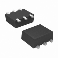
MOSFET P-CH DUAL 60V SOT563F
Manufacturer
Vishay
Datasheet
1.SI1026X-T1-GE3.pdf
(5 pages)
Specifications of SI1026X-T1-E3
Fet Type
2 N-Channel (Dual)
Fet Feature
Logic Level Gate
Rds On (max) @ Id, Vgs
1.4 Ohm @ 500mA, 10V
Drain To Source Voltage (vdss)
60V
Current - Continuous Drain (id) @ 25° C
305mA
Vgs(th) (max) @ Id
2.5V @ 250µA
Gate Charge (qg) @ Vgs
0.6nC @ 4.5V
Input Capacitance (ciss) @ Vds
30pF @ 25V
Power - Max
250mW
Mounting Type
Surface Mount
Package / Case
SC-89-6, SOT-563F, SOT-666
Transistor Polarity
N Channel
Continuous Drain Current Id
500mA
Drain Source Voltage Vds
60V
On Resistance Rds(on)
3ohm
Rds(on) Test Voltage Vgs
10V
Threshold Voltage Vgs Typ
2.5V
Lead Free Status / RoHS Status
Lead free / RoHS Compliant
Other names
SI1026X-T1-E3TR
Available stocks
Company
Part Number
Manufacturer
Quantity
Price

Part Number:
SI1026X-T1-E3
Manufacturer:
VISHAY/威世
Quantity:
20 000


Si1026X
Vishay Siliconix
Notes:
a. Pulse test; pulse width 300 µs, duty cycle 2 %.
b. For DESIGN AID ONLY, not subject to production testing.
c. Switching time is essentially independent of operating temperature.
Stresses beyond those listed under “Absolute Maximum Ratings” may cause permanent damage to the device. These are stress ratings only, and functional operation
of the device at these or any other conditions beyond those indicated in the operational sections of the specifications is not implied. Exposure to absolute maximum
rating conditions for extended periods may affect device reliability.
www.vishay.com
2
SPECIFICATIONS (T
Parameter
Static
Drain-Source Breakdown Voltage
Gate Threshold Voltage
Gate-Body Leakage
Zero Gate Voltage Drain Current
On-State Drain Current
Drain-Source On-Resistance
Forward Transconductance
Diode Forward Voltage
Dynamic
Total Gate Charge
Gate-Source Charge
Gate-Drain Charge
Input Capacitance
Output Capacitance
Reverse Transfer Capacitance
Switching
Turn-On Time
Turn-Off Time
b
b, c
a
a
a
a
J
= 25 °C, unless otherwise noted)
Symbol
R
V
I
I
I
C
V
D(on)
DS(on)
V
C
GS(th)
Q
Q
C
t
t
GSS
DSS
g
Q
(on)
(off)
DS
SD
oss
iss
rss
gd
fs
gs
g
V
V
I
D
DS
GS
V
= 200 mA, V
DS
= 10 V, I
= 10 V, I
V
V
V
= 60 V, V
V
V
V
V
V
V
V
V
DS
V
GS
V
DS
GS
DS
DS
DS
DD
DS
GS
DS
DS
GS
Test Conditions
= V
= 4.5 V, I
= 10 V, I
= 10 V, I
= 0 V, V
= 10 V, V
= 7.5 V, V
= 30 V, R
= 0 V, V
= 0 V, I
= 60 V, V
= 25 V, V
= 0 V, I
D
D
f = 1 MHz
GS
= 500 mA, T
= 250 mA, V
GEN
GS
, I
= 0 V, T
D
S
GS
D
D
D
GS
D
= 10 V, R
GS
= 200 mA
= 0.25 mA
L
GS
= 500 mA
= 200 mA
GS
GS
= 200 mA
= 10 µA
= ± 10 V
= 150
= ± 5 V
= 4.5 V
= 10 V
= 0 V
= 0 V,
J
J
GS
= 85 °C
= 125 °C
g
= 4.5 V
= 10
Min.
500
800
60
1
Typ.
200
600
120
225
30
15
20
6
3
S10-2432-Rev. D, 25-Oct-10
Document Number: 71434
± 150
Max.
± 50
1.40
2.50
1.40
2.5
3.0
10
1
Unit
mA
mS
nA
µA
pC
pF
ns
V
V
Related parts for SI1026X-T1-E3
Image
Part Number
Description
Manufacturer
Datasheet
Request
R

Part Number:
Description:
Manufacturer:
Vishay Semiconductors
Datasheet:

Part Number:
Description:
N-channel 60-v D-s Mosfet
Manufacturer:
Vishay
Datasheet:

Part Number:
Description:
MOSFET DL N-CH 60V 305MA SC89-6
Manufacturer:
Vishay
Datasheet:
Part Number:
Description:
357-036-542-201 CARDEDGE 36POS DL .156 BLK LOPRO
Manufacturer:
Vishay
Datasheet:
Part Number:
Description:
357-036-542-201 CARDEDGE 36POS DL .156 BLK LOPRO
Manufacturer:
Vishay
Datasheet:
Part Number:
Description:
357-036-542-201 CARDEDGE 36POS DL .156 BLK LOPRO
Manufacturer:
Vishay
Datasheet:
Part Number:
Description:
357-036-542-201 CARDEDGE 36POS DL .156 BLK LOPRO
Manufacturer:
Vishay
Datasheet:
Part Number:
Description:
357-036-542-201 CARDEDGE 36POS DL .156 BLK LOPRO
Manufacturer:
Vishay
Datasheet:
Part Number:
Description:
357-036-542-201 CARDEDGE 36POS DL .156 BLK LOPRO
Manufacturer:
Vishay
Datasheet:
Part Number:
Description:
357-036-542-201 CARDEDGE 36POS DL .156 BLK LOPRO
Manufacturer:
Vishay
Datasheet:
Part Number:
Description:
357-036-542-201 CARDEDGE 36POS DL .156 BLK LOPRO
Manufacturer:
Vishay
Datasheet:
Part Number:
Description:
357-036-542-201 CARDEDGE 36POS DL .156 BLK LOPRO
Manufacturer:
Vishay
Datasheet:
Part Number:
Description:
357-036-542-201 CARDEDGE 36POS DL .156 BLK LOPRO
Manufacturer:
Vishay
Datasheet:
Part Number:
Description:
357-036-542-201 CARDEDGE 36POS DL .156 BLK LOPRO
Manufacturer:
Vishay
Datasheet:
Part Number:
Description:
357-036-542-201 CARDEDGE 36POS DL .156 BLK LOPRO
Manufacturer:
Vishay
Datasheet: