2N5461RLRA ON Semiconductor, 2N5461RLRA Datasheet
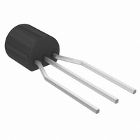
IC AMP JFET SS P-CH 40V TO-92

2N5461RLRA

Manufacturer Part Number
2N5461RLRA
Description
IC AMP JFET SS P-CH 40V TO-92
Manufacturer
ON Semiconductor
Datasheet

Specifications of 2N5461RLRA

Current - Drain (idss) @ Vds (vgs=0)
2mA @ 15V
Fet Type
P-Channel
Voltage - Breakdown (v(br)gss)
40V
Voltage - Cutoff (vgs Off) @ Id
1V @ 1µA
Input Capacitance (ciss) @ Vds
7pF @ 15V
Mounting Type
Through Hole
Package / Case
TO-92-3 (Standard Body), TO-226
Power - Max
350mW
Lead Free Status / RoHS Status
Contains lead / RoHS non-compliant
2N5460, 2N5461, 2N5462
JFET Amplifier
P−Channel − Depletion
Features
Stresses exceeding Maximum Ratings may damage the device. Maximum
Ratings are stress ratings only. Functional operation above the Recommended
Operating Conditions is not implied. Extended exposure to stresses above the
Recommended Operating Conditions may affect device reliability.
*For additional information on our Pb−Free strategy and soldering details, please
© Semiconductor Components Industries, LLC, 2006
March, 2006 − Rev. 5
MAXIMUM RATINGS
download the ON Semiconductor Soldering and Mounting Techniques
Reference Manual, SOLDERRM/D.
Drain − Gate Voltage
Reverse Gate − Source Voltage
Forward Gate Current
Total Device Dissipation @ T
Derate above 25°C
Junction Temperature Range
Storage Channel Temperature Range
Pb−Free Packages are Available*
Rating
A
= 25°C
Symbol
V
V
I
T
P
G(f)
GSR
T
DG
stg
D
J
−65 to +135
−65 to +150
Value
350
2.8
40
40
10
1
mW/°C
mAdc
Unit
Vdc
Vdc
mW
°C
°C
See detailed ordering and shipping information in the package
dimensions section on page 2 of this data sheet.
Preferred devices are recommended choices for future use
and best overall value.
(Note: Microdot may be in either location)
ORDERING INFORMATION
2N546x = Device Code
A
Y
WW
G
1 2
GATE
MARKING DIAGRAM
http://onsemi.com
3
3
= Assembly Location
= Year
= Work Week
= Pb−Free Package
x = 0, 1, or 2
AYWWG
546x
2N
G
Publication Order Number:
CASE 29
STYLE 7
1 SOURCE
TO−92
2 DRAIN
2N5460/D

Related parts for 2N5461RLRA

2N5461RLRA Summary of contents

Page 1

... Operating Conditions is not implied. Extended exposure to stresses above the Recommended Operating Conditions may affect device reliability. *For additional information on our Pb−Free strategy and soldering details, please download the ON Semiconductor Soldering and Mounting Techniques Reference Manual, SOLDERRM/D. © Semiconductor Components Industries, LLC, 2006 March, 2006 − ...

Page 2

... ORDERING INFORMATION Device 2N5460 2N5460G 2N5461 2N5461G 2N5461RLRA 2N5461RLRAG 2N5462 2N5462G †For information on tape and reel specifications, including part orientation and tape sizes, please refer to our Tape and Reel Packaging Specifications Brochure, BRD8011/D. 2N5460, 2N5461, 2N5462 (T = 25°C unless otherwise noted) ...

Page 3

DRAIN CURRENT versus GATE SOURCE VOLTAGE 4.0 3.5 3.0 2 −55°C 2.0 A 25°C 1.5 125°C 1.0 0 0.2 0.4 0.6 0.8 1.0 1 GATE−SOURCE VOLTAGE (VOLTS) GS Figure 2.0 V ...

Page 4

I , DRAIN CURRENT (mA) D Figure 7. Output Resistance versus Drain Current 10 9.0 8.0 7.0 6.0 5.0 4.0 3.0 2.0 1.0 0 ...

Page 5

... ISSUE SECTION X−X N. American Technical Support: 800−282−9855 Toll Free USA/Canada Japan: ON Semiconductor, Japan Customer Focus Center 2−9−1 Kamimeguro, Meguro−ku, Tokyo, Japan 153−0051 Phone: 81−3−5773−3850 http://onsemi.com 5 NOTES: 1. DIMENSIONING AND TOLERANCING PER ANSI Y14.5M, 1982. ...

Related keywords