MMBFU310LT1 ON Semiconductor, MMBFU310LT1 Datasheet

JFET SS N-CHAN 25V SOT23

MMBFU310LT1

Manufacturer Part Number
MMBFU310LT1
Description
JFET SS N-CHAN 25V SOT23
Manufacturer
ON Semiconductor
Datasheet

Specifications of MMBFU310LT1

Current - Drain (idss) @ Vds (vgs=0)
24mA @ 10V
Drain To Source Voltage (vdss)
25V
Fet Type
N-Channel
Voltage - Breakdown (v(br)gss)
25V
Voltage - Cutoff (vgs Off) @ Id
2.5V @ 1nA
Input Capacitance (ciss) @ Vds
5pF @ 10V (VGS)
Mounting Type
Surface Mount
Package / Case
TO-236-3, SC-59, SOT-23-3
Power - Max
225mW
Lead Free Status / RoHS Status
Contains lead / RoHS non-compliant
Other names
MMBFU310LT1OSCT

Available stocks

Company
Part Number
Manufacturer
Quantity
Price
Part Number:
MMBFU310LT1
Manufacturer:
FAIRCHILD
Quantity:
2 099
Part Number:
MMBFU310LT1
Manufacturer:
ON/安森美
Quantity:
20 000
Part Number:
MMBFU310LT1G
Manufacturer:
ON Semiconductor
Quantity:
4 450
Part Number:
MMBFU310LT1G
Manufacturer:
ON
Quantity:
30 000
Part Number:
MMBFU310LT1G
Manufacturer:
ON/安森美
Quantity:
20 000
MMBFU310LT1G
JFET Transistor
N−Channel
Features
Stresses exceeding Maximum Ratings may damage the device. Maximum
Ratings are stress ratings only. Functional operation above the Recommended
Operating Conditions is not implied. Extended exposure to stresses above the
Recommended Operating Conditions may affect device reliability.
1. FR−5 = 1.0  0.75  0.062 in.
© Semiconductor Components Industries, LLC, 2011
February, 2011 − Rev. 5
MAXIMUM RATINGS
THERMAL CHARACTERISTICS
Drain−Source Voltage
Gate−Source Voltage
Gate Current
Total Device Dissipation FR− 5 Board
Thermal Resistance,
Junction and Storage Temperature
Compliant
These Devices are Pb−Free, Halogen Free/BFR Free and are RoHS
(Note 1)
T
Derate above 25°C
Junction−to−Ambient
A
= 25°C
Rating
Symbol
T
R
J
V
V
P
, T
I
qJA
DS
GS
G
D
stg
−55 to +150
Value
225
556
1.8
25
25
10
1
mW/°C
mAdc
°C/W
Unit
Vdc
Vdc
mW
°C
†For information on tape and reel specifications,
MMBFU310LT1G
including part orientation and tape sizes, please
refer to our Tape and Reel Packaging Specifications
Brochure, BRD8011/D.
*Date Code orientation and/or overbar may
vary depending upon manufacturing location.
Device
(Note: Microdot may be in either location)
1
ORDERING INFORMATION
2
GATE
M6C = Device Code
M
G
MARKING DIAGRAM
3
http://onsemi.com
3
1
= Date Code*
= Pb−Free Package
(Pb−Free)
M6C M G
Package
SOT−23
SOT−23 (TO−236AB)
G
Publication Order Number:
CASE 318−08
1 DRAIN
2 SOURCE
STYLE 10
3000 Tape & Reel
MMBFU310LT1/D
Shipping

Related parts for MMBFU310LT1

MMBFU310LT1 Summary of contents

Page 1

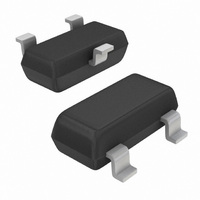
... ORDERING INFORMATION Device Package Shipping MMBFU310LT1G SOT−23 3000 Tape & Reel (Pb−Free) †For information on tape and reel specifications, including part orientation and tape sizes, please refer to our Tape and Reel Packaging Specifications Brochure, BRD8011/D. Publication Order Number: MMBFU310LT1/D † ...

Page 2

ELECTRICAL CHARACTERISTICS Characteristic OFF CHARACTERISTICS Gate−Source Breakdown Voltage − −1.0 mAdc Gate 1 Leakage Current − −15 Vdc Gate 2 Leakage Current − −15 Vdc Gate Source Cutoff ...

Page 3

1.0 k GS(off GS(off) 100 0.01 0.1 0.2 0.3 0.5 1.0 2.0 3.0 5 100 I , DRAIN CURRENT (mA) D Figure 3. Common−Source Output Admittance and ...

Page 4

... ON Semiconductor Website: www.onsemi.com Order Literature: http://www.onsemi.com/orderlit For additional information, please contact your local Sales Representative MMBFU310LT1/D ...

Related keywords