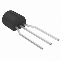
J112RLRAG ON Semiconductor, J112RLRAG Datasheet - Page 4

J112RLRAG
Manufacturer Part Number
J112RLRAG
Description
TRANS GP JFET N-CH 35V TO-92
Manufacturer
ON Semiconductor
Datasheet
1.J112G.pdf
(5 pages)
Specifications of J112RLRAG
Current - Drain (idss) @ Vds (vgs=0)
5mA @ 15V
Fet Type
N-Channel
Voltage - Breakdown (v(br)gss)
35V
Voltage - Cutoff (vgs Off) @ Id
1V @ 1µA
Resistance - Rds(on)
50 Ohm
Mounting Type
Through Hole
Package / Case
TO-92-3 (Standard Body), TO-226
Power - Max
350mW
Configuration
Single
Transistor Polarity
N-Channel
Gate-source Breakdown Voltage
35 V
Drain Current (idss At Vgs=0)
5 mA
Mounting Style
Through Hole
Breakdown Voltage Vbr
35V
Gate-source Cutoff Voltage Vgs(off) Max
-5V
Power Dissipation Pd
350mW
Operating Temperature Range
-65°C To +150°C
No. Of Pins
3
Leaded Process Compatible
Yes
Rohs Compliant
Yes
Lead Free Status / RoHS Status
Lead free / RoHS Compliant
Available stocks
Company
Part Number
Manufacturer
Quantity
Price
Company:
Part Number:
J112RLRAG()
Manufacturer:
MOT
Quantity:
2 059
200
160
120
7.0
5.0
3.0
2.0
100
20
10
80
40
90
80
70
60
50
40
30
20
10
0
0
0.5 0.7
10
0
Figure 6. Typical Forward Transfer Admittance
I
= 10
DSS
mA
20 30
Figure 10. Effect of I
Figure 8. Effect of Gate−Source Voltage
I
1.0
DSS
r
Resistance and Gate−Source Voltage
DS(on)
1.0
mA
25
, ZERO−GATE−VOLTAGE DRAIN CURRENT (mA)
V
On Drain−Source Resistance
40 50 60
T
GS
@ V
channel
2.0
J113
50 mA
, GATE−SOURCE VOLTAGE (VOLTS)
T
V
GS
2.0 3.0
channel
DS
I
D
= 0
= 25°C
, DRAIN CURRENT (mA)
= 15 V
3.0
75 mA 100 mA
= 25°C
70 80 90 100 110 120 130 140 150
5.0 7.0 10
4.0
DSS
On Drain−Source
5.0
J112
125 mA
V
T
6.0
channel
GS(off)
J111
20
http://onsemi.com
= 25°C
7.0
30
J111, J112
50
8.0
4
10
9.0
8.0
7.0
6.0
5.0
4.0
3.0
2.0
1.0
0
7.0
5.0
3.0
2.0
1.5
1.0
2.0
1.8
1.6
1.4
1.2
0.8
0.6
1.0
0.4
15
10
0.03 0.05 0.1
−70
The Zero−Gate−Voltage Drain Current (I
principle determinant of other J-FET characteristics.
Figure 10 shows the relationship of Gate−Source Off
Voltage (V
(r
of the values shown in Figure 10. This data will be useful
in predicting the characteristic variations for a given part
number.
The electrical characteristics table indicates that an J112
has an I
r
I
and 4.8 V.
ds(on)
DSS
ds(on)
For example:
Unknown
I
V
= 75 mA. The corresponding V
D
−40
GS
= 52 W for I
) to I
= 1.0 mA
r
Drain−Source On−State Resistance
ds(on)
Figure 9. Effect of Temperature On
DSS
= 0
Figure 7. Typical Capacitance
DSS
T
GS(off)
channel
range of 25 to 75 mA. Figure 10, shows
−10
and V
V
. Most of the devices will be within ±10%
T
(C
R
channel
, REVERSE VOLTAGE (VOLTS)
ds
, CHANNEL TEMPERATURE (°C)
0.3 0.5
IS NEGLIGIBLE)
and Drain−Source On Resistance
GS
20
= 25°C
DSS
range for an J112
NOTE 2
= 25 mA and 30 W for
1.0
50
C
C
gd
gs
80
3.0 5.0
GS
values are 2.2 V
110
DSS
10
), is the
140
170
30


