IXGX35N120BD1 IXYS, IXGX35N120BD1 Datasheet - Page 2
IXGX35N120BD1
Manufacturer Part Number
IXGX35N120BD1
Description
IGBT 70A 1200V PLUS247
Manufacturer
IXYS
Series
HiPerFAST™r
Datasheet
1.IXGK35N120B.pdf
(2 pages)
Specifications of IXGX35N120BD1
Voltage - Collector Emitter Breakdown (max)
1200V
Vce(on) (max) @ Vge, Ic
3.3V @ 15V, 35A
Current - Collector (ic) (max)
70A
Power - Max
350W
Input Type
Standard
Mounting Type
Through Hole
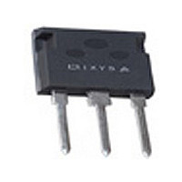
Package / Case
PLUS247™-3
Channel Type
N
Configuration
Single
Collector-emitter Voltage
1.2kV
Collector Current (dc) (max)
70A
Gate To Emitter Voltage (max)
±20V
Package Type
PLUS 247
Pin Count
3 +Tab
Mounting
Through Hole
Operating Temperature (min)
-55
Operating Temperature (max)
150C
Operating Temperature Classification
Military
Vces, (v)
1200
Ic25, Tc=25°c, Igbt, (a)
70
Ic90, Tc=90°c, Igbt, (a)
35
Ic110, Tc=110°c, Igbt, (a)
-
Vce(sat), Max, Tj=25°c, Igbt, (v)
3.3
Tfi, Typ, Tj=25°c, Igbt, (ns)
160
Eoff, Typ, Tj=125°c, Igbt, (mj)
8
Rthjc, Max, Igbt, (°c/w)
0.35
If, Tj=110°c, Diode, (a)
35
Rthjc, Max, Diode, (ºc/w)
0.65
Package Style
PLUS247
Lead Free Status / RoHS Status
Lead free / RoHS Compliant
Igbt Type
-
Lead Free Status / Rohs Status
Compliant


IXYS reserves the right to change limits, test conditions, and dimensions.
Reverse Diode (FRED)
Symbol
V
I
t
R
IXYS MOSFETS and IGBTs are covered by one or more of the following U.S. patents:
Symbol
g
C
C
C
Q
Q
Q
t
t
t
t
E
t
t
E
t
t
E
R
R
RM
d(on)
d(off)
d(on)
d(off)
rr
ri
fi
ri
fi
fs
off
on
off
F
thJC
thJC
thCK
ies
oes
res
g
ge
gc
Remarks: Switching times may
increase for V
higher T
Test Conditions
I
t ≤ 300 µs, duty cycle d ≤ 2 %, T
I
V
I
Test Conditions
I
Pulse test, t ≤ 300 µs, duty cycle ≤ 2 %
V
I
Inductive load, T
I
V
Remarks: Switching times may
increase for V
higher T
Inductive load, T
I
V
C
C
F
F
F
C
C
CE
R
CE
CE
= I
= I
= 1 A; -di/dt = 200 A/µs; V
= I
= I
= I
= 540 V
= 25 V, V
= 0.8 V
= 0.8 V
C90
C90
C90
= I
C90
C90
, V
, V
, V
, V
, V
C90
J
J
GE
GE
; V
GE
GE
GE
or increased R
or increased R
CES
CES
= 0 V, -di
= 0 V, Pulse test,
= 15 V, V
= 15 V
= 15 V
CE
GE
, R
, R
CE
CE
= 10 V,
= 0 V, f = 1 MHz
(Clamp) > 0.8 • V
G
(Clamp) > 0.8 • V
G
J
J
= R
= R
= 25° ° ° ° ° C
= 125° ° ° ° ° C
F
CE
/dt = 480 A/µs
off
off
= 0.5 V
= 5 Ω
= 5 Ω
G
G
R
= 30 V T
(T
(T
CES
J
J
J
= 25°C, unless otherwise specified)
= 25°C, unless otherwise specified)
= 125°C
CES
CES
,
,
T
J
J
=100°C
= 25°C
IXGK 35N120B
IXGX 35N120B
min.
min.
30
Characteristic Values
Characteristic Values
4,835,592
4,850,072
4620
0.15
225
typ.
typ.
260
170
180
160
300
360
3.8
2.6
8.0
32
40
40
90
28
57
50
27
55
31
4,881,106
4,931,844
max.
max.
2.35
0.65 K/W
0.35 K/W
280
320
7.3 mJ
36
60
5,017,508
5,034,796
K/W
mJ
mJ
nC
nC
nC
n s
n s
pF
pF
pF
n s
n s
n s
n s
n s
n s
n s
n s
S
V
A
PLUS247
TO-264 AA Outline (IXGK)
5,049,961
5,063,307
Terminals:
IXGK
IXGX
Dim.
A
A
A
b
b
b
C
D
E
e
L
L1
Q
R
Dim.
1
2
A
A1
A2
b
b1
b2
c
D
E
e
J
K
L
L1
P
Q
Q1
R
R1
S
T
1
2
20.80
15.75
19.81
TM
Min.
4.83
2.29
1.91
1.14
1.91
2.92
0.61
3.81
5.59
4.32
25.91
19.81
20.32
Min.
Millimeter
5.45 BSC
4.82
2.54
2.00
1.12
2.39
2.90
0.53
0.00
0.00
2.29
3.17
6.07
8.38
3.81
1.78
6.04
1.57
1 - Gate
2 - Drain (Collector)
3 - Source (Emitter)
4 - Drain (Collector)
5,187,117
Millimeter
5,237,481
Outline (IXGX)
5.46 BSC
21.34
16.13
20.32
Max.
35N120BD1
35N120BD1
26.16
19.96
20.83
5.21
2.54
2.16
1.40
2.13
3.12
0.80
4.32
6.20
4.83
Max.
5.13
2.89
2.10
1.42
2.69
3.09
0.83
0.25
0.25
2.59
3.66
6.27
8.69
4.32
2.29
6.30
1.83
5,486,715
5,381,025
Min.
1.020
Min. Max.
.190
.090
.075
.045
.075
.115
.024
.819
.620
.780
.150
.220 0.244
.170
.215 BSC
.780
.800
.190
.100
.079
.044
.094
.114
.021
.000
.000
.090
.125
.239
.330
.150
.070
.238
.062
Inches
.215 BSC
Inches
.205
.100
.085
.055
.084
.123
.031
.840
.635
.800
.170
.190
Max.
1.030
.202
.114
.083
.056
.106
.122
.033
.786
.010
.010
.820
.102
.144
.247
.342
.170
.090
.248
.072
6,306,728B1
Related parts for IXGX35N120BD1
Image
Part Number
Description
Manufacturer
Datasheet
Request
R


Part Number:
Description:
HiPerFET Power MOSFETs
Manufacturer:
IXYS Corporation
Datasheet:
Part Number:
Description:
J-K-Type Flip-Flop
Manufacturer:
IXYS Corporation
Datasheet:
Part Number:
Description:
HiPerRF Power MOSFETs
Manufacturer:
IXYS Corporation
Datasheet:
Part Number:
Description:
Rectifier Module for Three Phase Power Factor Correction
Manufacturer:
IXYS Corporation
Datasheet:
Part Number:
Description:
Thyristor Modules Thyristor/Diode Modules
Manufacturer:
IXYS Corporation
Datasheet:
Part Number:
Description:
Thyristor Modules Thyristor/Diode Modules
Manufacturer:
IXYS Corporation
Datasheet:
Part Number:
Description:
Thyristor Modules Thyristor/Diode Modules
Manufacturer:
IXYS Corporation
Datasheet:
Part Number:
Description:
Thyristor Modules Thyristor/Diode Modules
Manufacturer:
IXYS Corporation
Datasheet:
Part Number:
Description:
Thyristor Modules /Diode Modules
Manufacturer:
IXYS Corporation
Datasheet:
Part Number:
Description:
Thyristor Modules /Diode Modules
Manufacturer:
IXYS Corporation
Datasheet:
Part Number:
Description:
Thyristor Modules Thyristor/Diode Modules
Manufacturer:
IXYS Corporation
Datasheet: