MURA140T3G ON Semiconductor, MURA140T3G Datasheet - Page 4
MURA140T3G
Manufacturer Part Number
MURA140T3G
Description
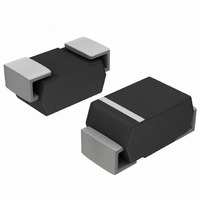
DIODE ULTRA FAST 1A 400V SMA
Manufacturer
ON Semiconductor
Datasheet
1.MURA140T3G.pdf
(4 pages)
Specifications of MURA140T3G
Voltage - Forward (vf) (max) @ If
1.1V @ 1A
Voltage - Dc Reverse (vr) (max)
400V
Current - Average Rectified (io)
2A
Current - Reverse Leakage @ Vr
5µA @ 400V
Diode Type
Standard
Speed
Fast Recovery =< 500ns, > 200mA (Io)
Reverse Recovery Time (trr)
65ns
Mounting Type
Surface Mount
Package / Case
DO-214AC, SMA
Product
Ultra Fast Recovery Rectifier
Configuration
Single
Reverse Voltage
400 V
Forward Voltage Drop
1.1 V @ 1 A
Recovery Time
65 ns
Forward Continuous Current
2 A
Max Surge Current
35 A
Reverse Current Ir
5 uA
Mounting Style
SMD/SMT
Maximum Operating Temperature
+ 175 C
Minimum Operating Temperature
- 65 C
Lead Free Status / RoHS Status
Lead free / RoHS Compliant
Capacitance @ Vr, F
-
Lead Free Status / Rohs Status
Lead free / RoHS Compliant
Other names
MURA140T3GOS
MURA140T3GOS
MURA140T3GOSTR
MURA140T3GOS
MURA140T3GOSTR
Available stocks
Company
Part Number
Manufacturer
Quantity
Price

Company:
Part Number:
MURA140T3G
Manufacturer:
ON Semiconductor
Quantity:
50
Part Number:
MURA140T3G
Manufacturer:
ON/安森美
Quantity:
20 000


PUBLICATION ORDERING INFORMATION
LITERATURE FULFILLMENT:
Literature Distribution Center for ON Semiconductor
P.O. Box 61312, Phoenix, Arizona 85082−1312 USA
Phone: 480−829−7710 or 800−344−3860 Toll Free USA/Canada
Fax: 480−829−7709 or 800−344−3867 Toll Free USA/Canada
Email: orderlit@onsemi.com
ON Semiconductor and
to any products herein. SCILLC makes no warranty, representation or guarantee regarding the suitability of its products for any particular purpose, nor does SCILLC assume any liability
arising out of the application or use of any product or circuit, and specifically disclaims any and all liability, including without limitation special, consequential or incidental damages.
“Typical” parameters which may be provided in SCILLC data sheets and/or specifications can and do vary in different applications and actual performance may vary over time. All
operating parameters, including “Typicals” must be validated for each customer application by customer’s technical experts. SCILLC does not convey any license under its patent rights
nor the rights of others. SCILLC products are not designed, intended, or authorized for use as components in systems intended for surgical implant into the body, or other applications
intended to support or sustain life, or for any other application in which the failure of the SCILLC product could create a situation where personal injury or death may occur. Should
Buyer purchase or use SCILLC products for any such unintended or unauthorized application, Buyer shall indemnify and hold SCILLC and its officers, employees, subsidiaries, affiliates,
and distributors harmless against all claims, costs, damages, and expenses, and reasonable attorney fees arising out of, directly or indirectly, any claim of personal injury or death
associated with such unintended or unauthorized use, even if such claim alleges that SCILLC was negligent regarding the design or manufacture of the part. SCILLC is an Equal
Opportunity/Affirmative Action Employer. This literature is subject to all applicable copyright laws and is not for resale in any manner.
L
H
E
E
POLARITY INDICATOR
OPTIONAL AS NEEDED
(SEE STYLES)
are registered trademarks of Semiconductor Components Industries, LLC (SCILLC). SCILLC reserves the right to make changes without further notice
b
c
*For additional information on our Pb−Free strategy and soldering
details, please download the ON Semiconductor Soldering and
Mounting Techniques Reference Manual, SOLDERRM/D.
D
MURA130T3, MURA140T3
A1
N. American Technical Support: 800−282−9855 Toll Free
USA/Canada
Japan: ON Semiconductor, Japan Customer Focus Center
2−9−1 Kamimeguro, Meguro−ku, Tokyo, Japan 153−0051
Phone: 81−3−5773−3850
PACKAGE DIMENSIONS
SOLDERING FOOTPRINT*
http://onsemi.com
CASE 403D−02
ISSUE C
0.157
SMA
4.0
4
A
0.0787
NOTES:
2.0
1. DIMENSIONING AND TOLERANCING PER ANSI
2. CONTROLLING DIMENSION: INCH.
3. 403D−01 OBSOLETE, NEW STANDARD IS 403D−02.
Y14.5M, 1982.
STYLE 1:
SCALE 8:1
DIM
H
A1
PIN 1. CATHODE (POLARITY BAND)
A
b
c
D
E
L
E
2. ANODE
MIN
1.91
0.05
1.27
0.15
2.29
4.06
4.83
0.76
0.0787
2.0
MILLIMETERS
inches
mm
NOM
2.16
0.10
1.45
0.28
2.60
4.32
5.21
1.14
ON Semiconductor Website: http://onsemi.com
Order Literature: http://www.onsemi.com/litorder
For additional information, please contact your
local Sales Representative.
MAX
2.41
0.15
1.63
0.41
2.92
4.57
5.59
1.52
0.075
0.002
0.050
0.006
0.090
0.160
0.190
0.030
MIN
MURA130T3/D
INCHES
0.085
0.004
0.057
0.011
0.103
0.170
0.205
0.045
NOM
0.095
0.006
0.064
0.016
0.115
0.180
0.220
0.060
MAX
Related parts for MURA140T3G
Image
Part Number
Description
Manufacturer
Datasheet
Request
R

Part Number:
Description:
ON Semiconductor [VOLTAGE REGULATOR]
Manufacturer:
ON Semiconductor
Datasheet:
Part Number:
Description:
357-036-542-201 CARDEDGE 36POS DL .156 BLK LOPRO
Manufacturer:
ON Semiconductor
Datasheet:
Part Number:
Description:
357-036-542-201 CARDEDGE 36POS DL .156 BLK LOPRO
Manufacturer:
ON Semiconductor
Datasheet:
Part Number:
Description:
357-036-542-201 CARDEDGE 36POS DL .156 BLK LOPRO
Manufacturer:
ON Semiconductor
Datasheet:
Part Number:
Description:
357-036-542-201 CARDEDGE 36POS DL .156 BLK LOPRO
Manufacturer:
ON Semiconductor
Datasheet:
Part Number:
Description:
357-036-542-201 CARDEDGE 36POS DL .156 BLK LOPRO
Manufacturer:
ON Semiconductor
Datasheet:
Part Number:
Description:
357-036-542-201 CARDEDGE 36POS DL .156 BLK LOPRO
Manufacturer:
ON Semiconductor
Datasheet:
Part Number:
Description:
357-036-542-201 CARDEDGE 36POS DL .156 BLK LOPRO
Manufacturer:
ON Semiconductor
Datasheet:
Part Number:
Description:
357-036-542-201 CARDEDGE 36POS DL .156 BLK LOPRO
Manufacturer:
ON Semiconductor
Datasheet:
Part Number:
Description:
357-036-542-201 CARDEDGE 36POS DL .156 BLK LOPRO
Manufacturer:
ON Semiconductor
Datasheet:
Part Number:
Description:
357-036-542-201 CARDEDGE 36POS DL .156 BLK LOPRO
Manufacturer:
ON Semiconductor
Datasheet:
Part Number:
Description:
Manufacturer:
ON Semiconductor
Datasheet:
Part Number:
Description:
Manufacturer:
ON Semiconductor
Datasheet:
Part Number:
Description:
Manufacturer:
ON Semiconductor
Datasheet: