NSR0230P2T5G ON Semiconductor, NSR0230P2T5G Datasheet

DIODE SCHOTTKY 30V 200MA SOD-923

NSR0230P2T5G

Manufacturer Part Number
NSR0230P2T5G
Description
DIODE SCHOTTKY 30V 200MA SOD-923
Manufacturer
ON Semiconductor
Datasheet

Specifications of NSR0230P2T5G

Voltage - Forward (vf) (max) @ If
500mV @ 200mA
Voltage - Dc Reverse (vr) (max)
30V
Current - Average Rectified (io)
200mA (DC)
Current - Reverse Leakage @ Vr
10µA @ 10V
Diode Type
Schottky
Speed
Small Signal =< 200mA (Io), Any Speed
Mounting Type
Surface Mount
Package / Case
SOD-923
Product
Schottky Diodes
Peak Reverse Voltage
30 V
Forward Continuous Current
0.2 A
Max Surge Current
1 A
Configuration
Single
Forward Voltage Drop
0.5 V
Maximum Reverse Leakage Current
10 uA @ 10 V
Maximum Power Dissipation
200 mW
Operating Temperature Range
- 55 C to + 125 C
Mounting Style
SMD/SMT
Lead Free Status / RoHS Status
Lead free / RoHS Compliant
Reverse Recovery Time (trr)
-
Capacitance @ Vr, F
-
Lead Free Status / Rohs Status
Lead free / RoHS Compliant
Other names
NSR0230P2T5G
NSR0230P2T5GOSTR

Available stocks

Company
Part Number
Manufacturer
Quantity
Price
Part Number:
NSR0230P2T5G
Manufacturer:
ON Semiconductor
Quantity:
3 000
Part Number:
NSR0230P2T5G
Manufacturer:
ON
Quantity:
30 000
Part Number:
NSR0230P2T5G
Manufacturer:
ON/安森美
Quantity:
20 000
Part Number:
NSR0230P2T5G
0
Company:
Part Number:
NSR0230P2T5G
Quantity:
50
Company:
Part Number:
NSR0230P2T5G
Quantity:
210
Company:
Part Number:
NSR0230P2T5G
Quantity:
25 762
Part Number:
NSR0230P2T5G K
Manufacturer:
ON/安森美
Quantity:
20 000
NSR0230P2T5G
Schottky Barrier Diode
switching applications, circuit protection, and voltage clamping.
Extremely low forward voltage reduces conduction loss. Miniature
surface mount package is excellent for hand−held and portable
applications where space is limited.
Features
Stresses exceeding Maximum Ratings may damage the device. Maximum
Ratings are stress ratings only. Functional operation above the Recommended
Operating Conditions is not implied. Extended exposure to stresses above the
Recommended Operating Conditions may affect device reliability.
MAXIMUM RATINGS
THERMAL CHARACTERISTICS
© Semiconductor Components Industries, LLC, 2009
May, 2009 − Rev. 1
1. FR−5 Minimum Pad.
ELECTRICAL CHARACTERISTICS
Reverse Voltage
Forward Current DC
Forward Current Surge Peak
ESD Rating: Class 3B per Human Body Model
ESD Rating:
Total Device Dissipation FR−5 Board,
Derate above 25°C
Thermal Resistance, Junction−to−Ambient
Junction and Storage
Reverse Leakage
Forward Voltage
These Schottky barrier diodes are designed for high−speed
Extremely Fast Switching Speed
Extremely Low Forward Voltage 0.325 V (max) @ I
Low Reverse Current
This is a Pb−Free Device
(60 Hz, 1 cycle)
(Note 1) T
Temperature Range
(V
(I
(I
F
F
R
= 10 mA)
= 200 mA)
= 10 V)
Characteristic
Class C per Machine Model
A
Characteristic
= 25°C
Rating
Symbol
(T
V
I
R
A
F
= 25°C unless otherwise noted)
Symbol
Symbol
T
R
Min
I
J
FSM
V
P
, T
I
qJA
F
R
D
stg
Typ
−55 to
Value
+125
Max
200
200
600
1.0
2.0
F
30
= 10 mA
0.325
0.500
Max
10
1
mW/°C
°C/W
Unit
Unit
Vdc
mW
mA
°C
A
Unit
Vdc
mA
†For information on tape and reel specifications,
NSR0230P2T5G
including part orientation and tape sizes, please
refer to our Tape and Reel Packaging Specifications
Brochure, BRD8011/D.
2
CASE 514AA
Device
SOD−923
PLASTIC
K
(Character is rotated 270° clockwise)
M = Month Code
G
(Note: Microdot may be in either location)
ORDERING INFORMATION
= Specific Device Code*
= Pb−Free Package
BARRIER DIODE
30 V SCHOTTKY
CATHODE
http://onsemi.com
1
1
SOD−923
Package
Publication Order Number:
1
ANODE
MARKING
DIAGRAM
2
8000/Tape & Reel
K MG
2 mm Pitch
Shipping†
NSR0230P2/D
G
2

Related parts for NSR0230P2T5G

NSR0230P2T5G Summary of contents

Page 1

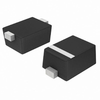
... Pb−Free Package (Note: Microdot may be in either location) ORDERING INFORMATION Device Package Shipping† NSR0230P2T5G SOD−923 2 mm Pitch 8000/Tape & Reel †For information on tape and reel specifications, including part orientation and tape sizes, please refer to our Tape and Reel Packaging Specifications Brochure, BRD8011/D ...

Page 2

T = 125°C A 100m T = 75°C A 10m 1m 100m T = 25°C A 10m T = −25° 0.1 0.2 0 FORWARD VOLTAGE (V) F Figure 1. Forward Characteristics ...

Page 3

... H E *For additional information on our Pb−Free strategy and soldering details, please download the ON Semiconductor Soldering and Mounting Techniques Reference Manual, SOLDERRM/D. ON Semiconductor and are registered trademarks of Semiconductor Components Industries, LLC (SCILLC). SCILLC reserves the right to make changes without further notice to any products herein. SCILLC makes no warranty, representation or guarantee regarding the suitability of its products for any particular purpose, nor does SCILLC assume any liability arising out of the application or use of any product or circuit, and specifically disclaims any and all liability, including without limitation special, consequential or incidental damages. “ ...

Related keywords