NSR0340HT1G ON Semiconductor, NSR0340HT1G Datasheet
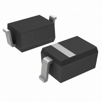
DIODE SCHOTTKY 40V 250MA SOD323

NSR0340HT1G

Manufacturer Part Number
NSR0340HT1G
Description
DIODE SCHOTTKY 40V 250MA SOD323
Manufacturer
ON Semiconductor
Datasheet

Specifications of NSR0340HT1G

Voltage - Forward (vf) (max) @ If
590mV @ 200mA
Voltage - Dc Reverse (vr) (max)
40V
Current - Average Rectified (io)
250mA (DC)
Current - Reverse Leakage @ Vr
6µA @ 40V
Diode Type
Schottky
Speed
Fast Recovery =< 500ns, > 200mA (Io)
Reverse Recovery Time (trr)
5ns
Capacitance @ Vr, F
6pF @ 10V, 1MHz
Mounting Type
Surface Mount
Package / Case
SC-76, SOD-323, UMD2
Product
Schottky Diodes
Peak Reverse Voltage
40 V
Forward Continuous Current
0.25 A
Configuration
Single
Recovery Time
5 ns (Typ)
Forward Voltage Drop
0.59 V
Maximum Reverse Leakage Current
6 uA
Operating Temperature Range
- 55 C to + 150 C
Mounting Style
SMD/SMT
Lead Free Status / RoHS Status
Lead free / RoHS Compliant
Other names
NSR0340HT1GOSTR

Available stocks

Company
Part Number
Manufacturer
Quantity
Price
Part Number:
NSR0340HT1G
Manufacturer:
ON Semiconductor
Quantity:
30 320
Part Number:
NSR0340HT1G
Manufacturer:
ON/安森美
Quantity:
20 000
Part Number:
NSR0340HT1G
0
Company:
Part Number:
NSR0340HT1G
Quantity:
1 380
Company:
Part Number:
NSR0340HT1G
Quantity:
6 000
Company:
Part Number:
NSR0340HT1G
Quantity:
5 000
NSR0340HT1G
Schottky Barrier Diode
drop and low leakage current and are used in a wide range of dc−dc
converter, clamping and protection applications in portable devices.
NSR0340H in a SOD−323 miniature package enables designers to
meet the challenging task of achieving higher efficiency and meeting
reduced space requirements.
Features
Typical Applications
Markets
Stresses exceeding Maximum Ratings may damage the device. Maximum
Ratings are stress ratings only. Functional operation above the Recommended
Operating Conditions is not implied. Extended exposure to stresses above the
Recommended Operating Conditions may affect device reliability.
MAXIMUM RATINGS
© Semiconductor Components Industries, LLC, 2010
September, 2010 − Rev. 1
Reverse Voltage
Forward Continuous Current (DC)
ESD Rating: Human Body Model
Non−Repetitive Peak Forward Surge
Schottky barrier diodes are optimized for very low forward voltage
Compliant
Very Low Forward Voltage Drop −415 mV @ 100 mA
Low Reverse Current − 0.4 mA @ 25 V V
250 mA of Continuous Forward Current
Power Dissipation of 160 mW with Minimum Trace
Very High Switching Speed
Low Capacitance − C
These Devices are Pb−Free, Halogen Free/BFR Free and are RoHS
LCD and Keypad Backlighting
Camera Photo Flash
Buck and Boost dc−dc Converters
Reverse Voltage and Current Protection
Clamping & Protection
Mobile Handsets
MP3 Players
Digital Camera and Camcorders
Notebook PCs and PDAs
GPS
Current
Machine Model
Rating
T
= 6 pF
Symbol
ESD
I
FSM
V
I
F
R
R
Value
250
1.0
40
Class 2
Class A
1
Unit
Vdc
mA
A
*This package is inherently Pb−Free.
†For information on tape and reel specifications,
NSR0340HT1G
including part orientation and tape sizes, please
refer to our Tape and Reel Packaging Specifications
Brochure, BRD8011/D.
1
Device
CASE 477
AD = Specific Device Code
M
G
(Note: Microdot may be in either location)
SOD−323
STYLE 1
40 VOLT SCHOTTKY
CATHODE
ORDERING INFORMATION
= Date Code
= Pb−Free Package
BARRIER DIODE
1
http://onsemi.com
2
SOD−323*
(Pb−Free)
Package
Publication Order Number:
MARKING
DIAGRAM
ANODE
3000/Tape & Reel
2
AD MG
Shipping
NSR0340H/D
G

Related parts for NSR0340HT1G

NSR0340HT1G Summary of contents

Page 1

... Ratings are stress ratings only. Functional operation above the Recommended Operating Conditions is not implied. Extended exposure to stresses above the Recommended Operating Conditions may affect device reliability. © Semiconductor Components Industries, LLC, 2010 September, 2010 − Rev NSR0340HT1G Symbol Value Unit V 40 ...

Page 2

THERMAL CHARACTERISTICS Characteristic Thermal Resistance Junction−to−Ambient (Note 1) Total Power Dissipation @ T = 25°C A Thermal Resistance Junction−to−Ambient (Note 2) Total Power Dissipation @ T = 25°C A Junction and Storage Temperature Range 1. Mounted onto ...

Page 3

V , FORWARD VOLTAGE (V) F Figure 2. Forward Voltage 10000 150°C 1000 100 125°C 10 85°C ...

Page 4

... NOTE 5 NOTE 3 *For additional information on our Pb−Free strategy and soldering details, please download the ON Semiconductor Soldering and Mounting Techniques Reference Manual, SOLDERRM/D. ON Semiconductor and are registered trademarks of Semiconductor Components Industries, LLC (SCILLC). SCILLC reserves the right to make changes without further notice to any products herein ...

Related keywords