BAS21DW5T1G ON Semiconductor, BAS21DW5T1G Datasheet - Page 2
BAS21DW5T1G
Manufacturer Part Number
BAS21DW5T1G
Description
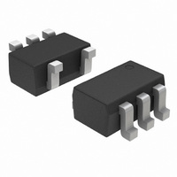
DIODE SWITCH 200MA 250V SOT353
Manufacturer
ON Semiconductor
Datasheet
1.BAS21DW5T1.pdf
(6 pages)
Specifications of BAS21DW5T1G
Voltage - Forward (vf) (max) @ If
1.25V @ 200mA
Current - Reverse Leakage @ Vr
100nA @ 200V
Current - Average Rectified (io) (per Diode)
200mA (DC)
Voltage - Dc Reverse (vr) (max)
250V
Reverse Recovery Time (trr)
50ns
Diode Type
Standard
Speed
Small Signal =< 200mA (Io), Any Speed
Diode Configuration
2 Independent
Mounting Type
Surface Mount
Package / Case
SC-70-5, SC-88A, SOT-323-5, SOT-353, 5-TSSOP
Product
Switching Diodes
Peak Reverse Voltage
250 V
Forward Continuous Current
0.2 A
Max Surge Current
0.625 A
Configuration
Dual Parallel
Recovery Time
50 ns
Forward Voltage Drop
1.25 V
Maximum Reverse Leakage Current
0.1 uA
Operating Temperature Range
- 55 C to + 150 C
Maximum Operating Temperature
+ 150 C
Minimum Operating Temperature
- 55 C
Mounting Style
SMD/SMT
Rectifier Type
Small Signal Switching Diode
Peak Rep Rev Volt
250V
Avg. Forward Curr (max)
0.2A
Rev Curr
0.1uA
Peak Non-repetitive Surge Current (max)
0.625A
Forward Voltage
1.25V
Operating Temp Range
-55C to 150C
Package Type
SC-70
Rev Recov Time
50ns
Operating Temperature Classification
Military
Mounting
Surface Mount
Pin Count
5
Lead Free Status / RoHS Status
Lead free / RoHS Compliant
Other names
BAS21DW5T1GOSTR
Available stocks
Company
Part Number
Manufacturer
Quantity
Price
Company:

Part Number:
BAS21DW5T1G
Manufacturer:
ON Semiconductor
Quantity:
28 975
Company:
Part Number:
BAS21DW5T1G
Manufacturer:
ON
Quantity:
30 000
Part Number:
BAS21DW5T1G
Manufacturer:
ON/安森美
Quantity:
20 000


THERMAL CHARACTERISTICS (SOT−23)
THERMAL CHARACTERISTICS (SC−88A)
2. FR−5 = 1.0
3. Alumina = 0.4
4. Mounted on FR−5 Board = 1.0 x 0.75 x 0.062 in.
ELECTRICAL CHARACTERISTICS
Thermal Resistance
Junction−to−Ambient (SOT−23)
Power Dissipation (Note 4)
Thermal Resistance −
Junction−to−Ambient
Derate Above 25°C
Operating Junction and Storage Temperature Range
Total Device Dissipation FR−5 Board
Total Device Dissipation Alumina Substrate
Thermal Resistance Junction−to−Ambient
Junction and Storage
Temperature Range
Maximum Junction Temperature
Reverse Voltage Leakage Current
Reverse Breakdown Voltage
Forward Voltage
Diode Capacitance (V
Reverse Recovery Time (I
(Note 2)
T
Derate above 25°C
(Note 3)
T
Derate above 25°C
(V
(V
(V
(V
(V
(V
(I
(I
(I
(I
(I
A
A
BR
BR
BR
F
F
R
R
R
R
R
R
= 25°C
= 25°C
= 100 mAdc)
= 200 mAdc)
= 100 Vdc)
= 150 Vdc)
= 200 Vdc)
= 100 Vdc, T
= 150 Vdc, T
= 200 Vdc, T
= 100 mAdc)
= 100 mAdc)
= 100 mAdc)
0.75
J
J
J
0.3
= 150°C)
= 150°C)
= 150°C)
R
= 0, f = 1.0 MHz)
0.062 in.
F
0.024 in. 99.5% alumina.
= I
Characteristic
R
Characteristic
Characteristic
= 30 mAdc, I
(T
A
= 25°C unless otherwise noted)
R(REC)
= 3.0 mAdc, R
http://onsemi.com
2
L
BAS19
BAS20
BAS21
BAS19
BAS20
BAS21
BAS19
BAS20
BAS21
= 100)
Symbol
Symbol
Symbol
T
T
T
V
R
R
R
J
J
P
P
P
Jmax
, T
, T
C
V
(BR)
qJA
qJA
qJA
I
t
R
rr
D
D
D
F
D
stg
stg
−55 to +150
−55 to +150
Min
120
200
250
−
−
−
−
−
−
−
−
−
−
Max
Max
225
556
300
417
385
328
150
1.8
2.4
3.0
Max
1.25
100
100
100
0.1
0.1
0.1
1.0
5.0
50
−
−
−
mW/°C
mW/°C
mW/°C
°C/W
°C/W
°C/W
Unit
Unit
mW
mW
mW
°C
°C
°C
mAdc
Unit
Vdc
Vdc
pF
ns
Related parts for BAS21DW5T1G
Image
Part Number
Description
Manufacturer
Datasheet
Request
R


Part Number:
Description:
ON Semiconductor [VOLTAGE REGULATOR]
Manufacturer:
ON Semiconductor
Datasheet:
Part Number:
Description:
357-036-542-201 CARDEDGE 36POS DL .156 BLK LOPRO
Manufacturer:
ON Semiconductor
Datasheet:
Part Number:
Description:
357-036-542-201 CARDEDGE 36POS DL .156 BLK LOPRO
Manufacturer:
ON Semiconductor
Datasheet:
Part Number:
Description:
357-036-542-201 CARDEDGE 36POS DL .156 BLK LOPRO
Manufacturer:
ON Semiconductor
Datasheet:
Part Number:
Description:
357-036-542-201 CARDEDGE 36POS DL .156 BLK LOPRO
Manufacturer:
ON Semiconductor
Datasheet:
Part Number:
Description:
357-036-542-201 CARDEDGE 36POS DL .156 BLK LOPRO
Manufacturer:
ON Semiconductor
Datasheet:
Part Number:
Description:
357-036-542-201 CARDEDGE 36POS DL .156 BLK LOPRO
Manufacturer:
ON Semiconductor
Datasheet:
Part Number:
Description:
357-036-542-201 CARDEDGE 36POS DL .156 BLK LOPRO
Manufacturer:
ON Semiconductor
Datasheet:
Part Number:
Description:
357-036-542-201 CARDEDGE 36POS DL .156 BLK LOPRO
Manufacturer:
ON Semiconductor
Datasheet:
Part Number:
Description:
357-036-542-201 CARDEDGE 36POS DL .156 BLK LOPRO
Manufacturer:
ON Semiconductor
Datasheet:
Part Number:
Description:
357-036-542-201 CARDEDGE 36POS DL .156 BLK LOPRO
Manufacturer:
ON Semiconductor
Datasheet:
Part Number:
Description:
Manufacturer:
ON Semiconductor
Datasheet:
Part Number:
Description:
Manufacturer:
ON Semiconductor
Datasheet: