MBR4015LWTG ON Semiconductor, MBR4015LWTG Datasheet

DIODE SCHOTTKY 15V 20A TO-247

MBR4015LWTG

Manufacturer Part Number
MBR4015LWTG
Description
DIODE SCHOTTKY 15V 20A TO-247
Manufacturer
ON Semiconductor
Series
SWITCHMODE™r
Datasheet

Specifications of MBR4015LWTG

Voltage - Forward (vf) (max) @ If
420mV @ 20A
Current - Reverse Leakage @ Vr
5mA @ 15V
Current - Average Rectified (io) (per Diode)
20A
Voltage - Dc Reverse (vr) (max)
15V
Diode Type
Schottky
Speed
Fast Recovery =< 500ns, > 200mA (Io)
Diode Configuration
1 Pair Common Cathode
Mounting Type
Through Hole, Radial
Package / Case
TO-247-3 (Straight Leads), TO-247AC
Product
Schottky Diodes
Peak Reverse Voltage
15 V
Forward Continuous Current
40 A
Max Surge Current
120 A
Configuration
Dual Common Cathode
Forward Voltage Drop
0.5 V
Maximum Reverse Leakage Current
5000 uA
Operating Temperature Range
- 55 C to + 150 C
Mounting Style
Through Hole
Lead Free Status / RoHS Status
Lead free / RoHS Compliant
Reverse Recovery Time (trr)
-
Lead Free Status / Rohs Status
Lead free / RoHS Compliant

Available stocks

Company
Part Number
Manufacturer
Quantity
Price
Part Number:
MBR4015LWTG
Manufacturer:
ON
Quantity:
12 500
MBR4015LWT
SWITCHMODEt
Schottky Power Rectifier
TO247 Power Package
metal−to−silicon power rectifier. Features epitaxial construction with
oxide passivation and metal overlay contact. Ideally suited for low
voltage, high frequency switching power supplies; free wheeling
diodes and polarity protection diodes.
Features
Mechanical Characteristics
Stresses exceeding Maximum Ratings may damage the device. Maximum
Ratings are stress ratings only. Functional operation above the Recommended
Operating Conditions is not implied. Extended exposure to stresses above the
Recommended Operating Conditions may affect device reliability.
*For additional information on our Pb−Free strategy and soldering details, please
MAXIMUM RATINGS
© Semiconductor Components Industries, LLC, 2010
March, 2010 − Rev. 9
download the ON Semiconductor Soldering and Mounting Techniques
Reference Manual, SOLDERRM/D.
Peak Repetitive Reverse Voltage
Average Rectified Forward Current
(At Rated V
Peak Repetitive Forward Current,
Non−Repetitive Peak Surge Current
Storage/Operating Case Temperature
Operating Junction Temperature (Note 1)
Voltage Rate of Change,
This device employs the Schottky Barrier principle in a large area
Parallel Operation at Full Rating.
Leads are Readily Solderable
260°C Max. for 10 Seconds
Highly Stable Oxide Passivated Junction
Guardring for Overvoltage Protection
Low Forward Voltage Drop
Dual Diode Construction; Terminals 1 and 3 May Be Connected for
Full Electrical Isolation without Additional Hardware
Pb−Free Package is Available*
Case: Molded Epoxy
Epoxy Meets UL 94 V−0 @ 0.125 in
Weight: 4.3 Grams (Approximately)
Finish: All External Surfaces Corrosion Resistant and Terminal
Lead and Mounting Surface Temperature for Soldering Purposes:
Working Peak Reverse Voltage
DC Blocking Voltage
(At Rated V
20 kHz, T
(Surge Applied at Rated Load
Conditions Halfwave, Single Phase,
60 Hz) Per Package
(Rated V
R
R
C
, T
, T
R
= 95°C)
, Square Wave,
J
C
= 25°C)
Rating
= 120°C)
Per Package
Per Leg
Per Leg
Symbol
T
V
V
stg
dv/dt
I
I
FRM
RWM
FSM
RRM
V
T
I
O
, T
R
J
C
−55 to +150
−55 to +150
10,000
Value
120
15
20
40
40
1
Unit
V/ms
°C
°C
V
A
A
A
MBR4015LWT
MBR4015LWTG
1
Device
MBR4015LWT = Specific Device Code
A
Y
WW
G
40 AMPERES, 15 VOLTS
2
SCHOTTKY BARRIER
ORDERING INFORMATION
3
MARKING DIAGRAM
http://onsemi.com
RECTIFIER
1
3
MBR4015LWT
(Pb−Free)
Package
TO−247
TO−247
AYWWG
= Assembly Location
= Year
= Work Week
= Pb−Free Package
Publication Order Number:
CASE 340L
STYLE 2
TO−247
MBR4015LWT/D
30 Units / Rail
30 Units / Rail
Shipping
2

Related parts for MBR4015LWTG

MBR4015LWTG Summary of contents

Page 1

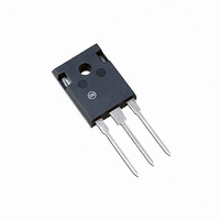
... FRM I 120 A FSM −55 to +150 °C stg C T −55 to +150 °C J dv/dt 10,000 V/ms MBR4015LWT MBR4015LWTG 1 http://onsemi.com SCHOTTKY BARRIER RECTIFIER 40 AMPERES, 15 VOLTS TO−247 1 CASE 340L 2 3 STYLE 2 MARKING DIAGRAM MBR4015LWT AYWWG MBR4015LWT = Specific Device Code A = Assembly Location Y = Year WW = Work Week G = Pb− ...

Page 2

THERMAL CHARACTERISTICS Rating Thermal Resistance, Junction−to−Case Junction−to−Ambient ELECTRICAL CHARACTERISTICS Rating Maximum Instantaneous Forward Voltage (Note 2), See Figure 2 Per Leg ( Maximum Instantaneous Reverse Current (Note 2), See Figure 4 ...

Page 3

DC 30 SQUAREWAVE CASE TEMPERATURE (°C) C Figure 5. Current Derating Per Leg 10,000 1000 100 0 2.0 4.0 6.0 8 REVERSE VOLTAGE (V) R Figure 7. ...

Page 4

Rtjl(t) = Rtjl*r(t) 0.01 0.00001 0.0001 Figure 9. Thermal Response Junction to Lead (Per Leg) 1.0 50% 20% 0.1 10% 5.0% 2.0% 0.01 1.0% 0.001 0.0001 0.00001 0.0001 0.001 Figure 10. Thermal ...

Page 5

... Opportunity/Affirmative Action Employer. This literature is subject to all applicable copyright laws and is not for resale in any manner. PUBLICATION ORDERING INFORMATION LITERATURE FULFILLMENT: Literature Distribution Center for ON Semiconductor P.O. Box 5163, Denver, Colorado 80217 USA Phone: 303−675−2175 or 800−344−3860 Toll Free USA/Canada Fax: 303− ...

Related keywords