MBRB41H100CTT4G ON Semiconductor, MBRB41H100CTT4G Datasheet
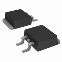
DIODE SCHOTTKY 100V 20A H D2PAK

MBRB41H100CTT4G

Manufacturer Part Number
MBRB41H100CTT4G
Description
DIODE SCHOTTKY 100V 20A H D2PAK
Manufacturer
ON Semiconductor
Series
SWITCHMODE™r
Datasheet

Specifications of MBRB41H100CTT4G

Voltage - Forward (vf) (max) @ If
800mV @ 20A
Current - Reverse Leakage @ Vr
10µA @ 100V
Current - Average Rectified (io) (per Diode)
20A
Voltage - Dc Reverse (vr) (max)
100V
Diode Type
Schottky
Speed
Fast Recovery =< 500ns, > 200mA (Io)
Diode Configuration
1 Pair Common Cathode
Mounting Type
Surface Mount
Package / Case
D²Pak, TO-263 (2 leads + tab)
Lead Free Status / RoHS Status
Lead free / RoHS Compliant
Reverse Recovery Time (trr)
-

Available stocks

Company
Part Number
Manufacturer
Quantity
Price
Part Number:
MBRB41H100CTT4G
Manufacturer:
ON
Quantity:
12 500
Part Number:
MBRB41H100CTT4G
Manufacturer:
ON/安森美
Quantity:
20 000
MBR41H100CT,
MBRB41H100CT,
MBRB41H100CT-1
SWITCHMODE]
Power Rectifier
100 V, 40 A
Features and Benefits
Applications
Mechanical Characteristics:
MAXIMUM RATINGS
© Semiconductor Components Industries, LLC, 2008
June, 2008 − Rev. 6
Please See the Table on the Following Page
Leads are Readily Solderable
260°C Max. for 10 Seconds
Low Forward Voltage: 0.67 V @ 125°C
Low Power Loss/High Efficiency
High Surge Capacity
175°C Operating Junction Temperature
40 A Total (20 A Per Diode Leg)
Guard−Ring for Stress Protection
Pb−Free Packages are Available
Power Supply − Output Rectification
Power Management
Instrumentation
Case: Epoxy, Molded
Epoxy Meets UL 94 V−0 @ 0.125 in
Weight (Approximately): 1.9 Grams (TO−220AB)
Finish: All External Surfaces Corrosion Resistant and Terminal
Lead Temperature for Soldering Purposes:
1.7 Grams (D
1.5 Grams (TO−262)
2
PAK)
1
1
†For information on tape and reel specifications,
MBR41H100CT
MBR41H100CTG
MBRB41H100CT−1G
MBRB41H100CTT4G
including part orientation and tape sizes, please
refer to our Tape and Reel Packaging Specifications
Brochure, BRD8011/D.
1
1 2
2
3
3
Device
3
4
ORDERING INFORMATION
4
http://onsemi.com
A
Y
WW
G
AKA
1
3
4
I
2
CASE 221A
TO−220AB
PAK (TO−262)
CASE 418D
PLASTIC
STYLE 6
PLASTIC
STYLE 3
CASE 418B
STYLE 3
D
(Pb−Free)
(Pb−Free)
(Pb−Free)
= Assembly Location
= Year
= Work Week
= Pb−Free Package
= Polarity Designator
Package
Publication Order Number:
2
TO−220
TO−220
TO−262
D
PAK
2
PAK
MBR41H100CT/D
2, 4
DIAGRAMS
MARKING
B41H100G
B41H100G
B41H100G
50 Units/Rail
50 Units/Rail
50 Units/Rail
800/Tape &
Shipping
AYWW
AYWW
AYWW
AKA
AKA
AKA
Reel

Related parts for MBRB41H100CTT4G

MBRB41H100CTT4G Summary of contents

Page 1

... Semiconductor Components Industries, LLC, 2008 June, 2008 − Rev PAK MBR41H100CT MBR41H100CTG MBRB41H100CT−1G MBRB41H100CTT4G †For information on tape and reel specifications, including part orientation and tape sizes, please refer to our Tape and Reel Packaging Specifications Brochure, BRD8011/D. 1 http://onsemi.com MARKING 4 DIAGRAMS TO− ...

Page 2

MAXIMUM RATINGS (Per Diode Leg) Peak Repetitive Reverse Voltage Working Peak Reverse Voltage DC Blocking Voltage Average Rectified Forward Current (Rated 150° Peak Repetitive Forward Current (Rated V , Square Wave, 20 kHz) T ...

Page 3

T = 150° 125° 25° 0.1 0 0.2 0.4 0 INSTANTANEOUS FORWARD VOLTAGE (VOLTS) F Figure 1. Typical Forward Voltage 1.0E−01 1.0E− 150°C J 1.0E−03 ...

Page 4

D = 0.5 0.2 10 0.1 0.05 1 0.01 0.1 0.01 SINGLE PULSE 0.001 0.000001 0.00001 0.0001 Figure 8. Thermal Response Junction−to−Ambient 0.5 1 0.2 0.1 0.05 0.1 0.01 0.01 SINGLE ...

Page 5

COIL MERCURY SWITCH DUT S 1 Figure 10. Test Circuit The unclamped inductive switching circuit shown in Figure 10 was used to demonstrate the controlled avalanche capability of this device. A mercury ...

Page 6

PACKAGE DIMENSIONS TO−220 CASE 221A−09 ISSUE AF NOTES: 1. DIMENSIONING AND TOLERANCING PER ANSI Y14.5M, 1982. SEATING −T− 2. CONTROLLING DIMENSION: INCH. ...

Page 7

... SEATING PLANE 0.13 (0.005 VARIABLE CONFIGURATION ZONE VIEW W−W VIEW W−W 1 10.66 0.42 *For additional information on our Pb−Free strategy and soldering details, please download the ON Semiconductor Soldering and Mounting Techniques Reference Manual, SOLDERRM/D. PACKAGE DIMENSIONS 2 D PAK 3 CASE 418B−04 ISSUE VIEW W− ...

Page 8

... Opportunity/Affirmative Action Employer. This literature is subject to all applicable copyright laws and is not for resale in any manner. PUBLICATION ORDERING INFORMATION LITERATURE FULFILLMENT: Literature Distribution Center for ON Semiconductor P.O. Box 5163, Denver, Colorado 80217 USA Phone: 303−675−2175 or 800−344−3860 Toll Free USA/Canada Fax: 303− ...

Related keywords