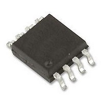
LT1999MPMS8-50#TRPBF Linear Technology, LT1999MPMS8-50#TRPBF Datasheet - Page 14

LT1999MPMS8-50#TRPBF
Manufacturer Part Number
LT1999MPMS8-50#TRPBF
Description
SC-Amps/Current Sense, High Voltage, Bidirectional Current Sense Amplifier
Manufacturer
Linear Technology
Datasheet
1.LT1999MPMS8-10PBF.pdf
(24 pages)
Specifications of LT1999MPMS8-50#TRPBF
Input Bias Current
137.5µA
Output Current Per Channel
26mA
Input Offset Voltage
1.5mV
Bandwidth
1.2MHz
Cmrr
120dB
Slew Rate
3V/µs
Supply Voltage Range
4.5V To 5.5V
Supply Current
3µA
Rohs Compliant
Yes
No. Of Amplifiers
2
Available stocks
Company
Part Number
Manufacturer
Quantity
Price
APPLICATIONS INFORMATION
LT1999-10/LT1999-20/
LT1999-50
The LT1999 current sense amplifi er provides accurate
bidirectional monitoring of current through a user-selected
sense resistor. The voltage generated by the current fl owing
in the sense resistor is amplifi ed by a fi xed gain of 10V/V,
20V/V or 50V/V (LT1999-10, LT1999-20, or LT1999-50
respectively) and is level shifted to the OUT pin. The volt-
age difference and polarity of the OUT pin with respect
to REF (Pin 6) indicates magnitude and direction of the
current in the sense resistor.
THEORY OF OPERATION
Refer to the Block Diagram (Figure 1).
Case 1: V
For input common mode voltages exceeding the power
supply, one can assume D1 of Figure 1 is completely off.
The sensed voltage (V
and Pin 3 (–IN) to matched resistors R
nally 4k each). The opposite ends of R
forced to equal potentials by transconductor G
convert the differentially sensed voltage into a sensed
current. The sensed current in R
level-shifted, and converted back into a voltage by trans-
resistance amplifi er A
provides high open loop gain to accurately convert the
sensed current back into a voltage and to drive external
loads. The theoretical output voltage is determined by
the sensed voltage (V
resistors:
where
For the LT1999-10, R
R
nally 200k.
14
G
R
V
is nominally 80k, and for the LT1999-50, R
OUT
IN
=
− V
R
+
+IN
< V
REF
+ R
2
CM
= V
< 80V
−IN
SENSE
G
SENSE
is nominally 40k. For the LT1999-20,
SENSE
O
nominally 4k
and resistor R
•
), and the ratio of two on-chip
) is applied across Pin 2 (+IN)
R
R
IN
G
+ IN
and R
+ IN
+ IN
– IN
G
and R
. Amplifi er A
and R
is combined,
– IN
G
IN
is nomi-
, which
(nomi-
– IN
are
O
The voltage difference between the OUT pin and the REF
pin represent both polarity and magnitude of the sensed
voltage. The noninverting input of amplifi er A
by a resistive 160k to 160k divider tied between V
GND to set the default REF pin bias to mid-supply.
Case 2: –5V < V
For common mode inputs which transition or are set
below the supply voltage, diode D1 will turn on and will
provide a source of current through R
the inputs of transconductance amplifi er G
above GND. The transition is smooth and continuous;
there are negligible changes to either gain or amplifi er
voltage offset. The only difference in amplifi er operation
is the bias currents provided by D1 through R
are steered through the input pins, otherwise amplifi er
operation is identical. The inputs to transconductance
amplifi er G
differential voltages appearing at the +IN and –IN pins into
a differential current. This differential current is combined,
level-shifted, and converted back into a voltage by trans-
resistance amplifi er A
and R
to prevent common mode to differential conversion from
occurring (to the extent of the matched trim) when the
input common mode transitions below V
As described in case 1, the output is determined by the
sense voltage and the ratio of two on-chip resistors:
where
R
V
OUT
IN
– S
=
are trimmed to match R
− V
R
IN
+IN
REF
are still forced to equal potentials forcing any
+ R
2
= V
CM
−IN
SENSE
< V
O
+
and Resistor R
•
R
R
IN
G
+ IN
and R
+S
G
– IN
and R
. Resistors R
+
IN
.
at least 2.25V
respectively,
+S
O
– S
is biased
and R
to bias
+
1999fa
and
– S
+S


