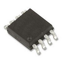
LT1999MPMS8-20#PBF Linear Technology, LT1999MPMS8-20#PBF Datasheet - Page 6

LT1999MPMS8-20#PBF
Manufacturer Part Number
LT1999MPMS8-20#PBF
Description
SC-Amps/Current Sense, High Voltage, Bidirectional Current Sense Amplifier
Manufacturer
Linear Technology
Datasheet
1.LT1999MPMS8-10PBF.pdf
(24 pages)
Specifications of LT1999MPMS8-20#PBF
Input Bias Current
137.5µA
Output Current Per Channel
26mA
Input Offset Voltage
1.5mV
Bandwidth
2MHz
Cmrr
120dB
Slew Rate
3V/µs
Supply Voltage Range
4.5V To 5.5V
Supply Current
3µA
Rohs Compliant
Yes
No. Of Amplifiers
2
Available stocks
Company
Part Number
Manufacturer
Quantity
Price
LT1999-10/LT1999-20/
LT1999-50
ELECTRICAL CHARACTERISTICS
temperature range, –55°C < T
V
SYMBOL
t
V
I
R
I
I
V
t
t
Note 1: Stresses beyond those listed under Absolute Maximum Ratings
may cause permanent damage to the device. Exposure to any Absolute
Maximum Rating condition for extended periods may affect device
reliability and lifetime.
Note 2: Pin 2 (+IN) and Pin 3 (–IN) are protected by ESD voltage clamps
which have asymmetric bidirectional breakdown characteristics with respect
to the GND pin (Pin 5). These pins can safely support common mode
voltages which vary from –5.25V to 88V without triggering an ESD clamp.
Note 3: Exposure to differential sense voltages exceeding the normal
operating range for extended periods of time may degrade part
performance. A heat sink may be required to keep the junction temperature
below the Absolute Maximum Rating when the inputs are stressed
differentially. The amount of power dissipated in the LT1999 due to input
overdrive can be approximated by:
Note 4: A heat sink may be required to keep the junction temperature
below the absolute maximum rating.
Note 5: The LT1999C/LT1999I are guaranteed functional over the operating
temperature range –40°C to 85°C. The LT1999H is guaranteed functional
over the operating temperature range –40°C to 125°C. The LT1999MP is
guaranteed functional over the operating temperature range –55°C to 150°C.
Junction temperatures greater than 125°C will promote accelerated aging.
The LT1999 has a demonstrated typical life beyond 1000 hours at 150°C.
Note 6: The LT1999C is guaranteed to meet specified performance from
0°C to 70°C. The LT1999C is designed, characterized, and expected to
meet specified performance from –40°C to 85°C but is not tested or
QA sampled at these temperatures. The LT1999I is guaranteed to meet
specified performance from –40°C to 85°C. The LT1999H is guaranteed
to meet specified performance from –40°C to 125°C. The LT1999MP is
guaranteed to meet specified performance from –55°C to 150°C.
6
r
S
SRC
SNK
ON
OFF
S
OUT
REF
O
= floating, V
P
PARAMETER
Common Mode Step Recovery Time
ΔV
(Note 10)
Supply Voltage (Note 11)
Supply Current
Output Impedance
Sourcing Output Current
Sinking Output Current
Swing Output High (with Respect to V
Swing Output Low (with Respect to V
Turn-On Time
Turn-Off Time
DISS
CM
=
= ±50V, 20ns
(
SHDN
V
+IN
8kΩ
− V
= floating, unless otherwise specified. See Figure 2.
−IN
)
2
A
< 150°C for MP-grade parts, otherwise specifications are at T
–
+
)
)
CONDITIONS
LT1999-10
LT1999-20
LT1999-50
V
V
V
ΔI
R
R
R
R
R
R
V
V
CM
CM
+
SHDN
SHDN
LOAD
LOAD
LOAD
LOAD
LOAD
LOAD
O
= 5.5V, V
The
= ±2mA
> 5.5V
= –5V
= 50Ω to GND
= 50Ω to V
= 1kΩ to Mid-Supply
= Open
= 1kΩ to Mid-Supply
= Open
= 0V to 5V
= 5V to 0V
l
denotes the specifications which apply over the full operating
SHDN
Note 7: Full-scale sense (V
differential input that can be applied with better than 0.5% gain accuracy.
Gain accuracy is degraded when the output saturates against either power
supply rail. V
set to it’s voltage range limits. The maximum V
REF pin set to it’s minimum specified limit, verifying the gain error is less
than 0.5% at the output. The minimum V
set to its maximum specified limit, verifying the gain error at the output is
less than 0.5%. See Note 9 for more information.
Note 8: I
and –IN pins (Pins 2 and 3). A positive current indicates current flowing
into the pin. I
I
Note 9: The REF pin voltage range is the minimum and maximum limits
that ensures the input referred voltage offset does not exceed ±3mV over
the I, C, and H temperature ranges, and ±3.5mV over the MP temperature
range.
Note 10: Common mode recovery time is defined as the time it takes the
output of the LT1999 to recover from a 50V, 20ns input common mode
voltage transition, and settle to within the DC amplifier specifications.
Note 11: Operating the LT1999 with V
LT1999 is not tested or specified in this condition. See the Applications
Information section.
OS
= 0.5V, V
+
= I(+IN) – I(–IN)
B
CM
is defined as the average of the input bias currents to the +IN
SENSE
> 0V
OS
is defined as the difference of the input bias currents.
is verified with V
l
l
l
l
l
l
l
l
l
l
SENSE
A
= 25°C. V
) gives indication of the maximum
MIN
4.5
10
3
+
= 5.5V, V
+
< 4.5V is possible, although the
+
SENSE
= 5V, GND = 0V, V
1.55
0.15
TYP
125
175
150
0.8
1.3
5.8
31
26
1
5
3
5
1
1
CM
SENSE
is verified with the REF pin
= 12V, with the REF pin
is verified with the
MAX
250
125
250
225
5.5
1.9
7.1
25
40
40
CM
= 12V,
UNITS
1999fa
mA
mA
mA
mA
mV
mV
mV
mV
μA
μs
μs
μs
μs
μs
Ω
V


