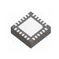
LM4946SQ National Semiconductor, LM4946SQ Datasheet - Page 22

LM4946SQ
Manufacturer Part Number
LM4946SQ
Description
IC,Audio Amplifier,TRIPLE,LLCC,24PIN,PLASTIC
Manufacturer
National Semiconductor
Datasheet
1.LM4946SQ.pdf
(32 pages)
Specifications of LM4946SQ
Operational Class
Class-AB
Audio Amplifier Output Configuration
1-Channel Mono/2-Channel Stereo
Audio Amplifier Function
Headphone/Speaker
Total Harmonic Distortion
0.05%%
Single Supply Voltage (typ)
3/5V
Dual Supply Voltage (typ)
Not RequiredV
Power Supply Requirement
Single
Rail/rail I/o Type
No
Power Supply Rejection Ratio
72dB
Single Supply Voltage (min)
2.7V
Single Supply Voltage (max)
5.5V
Dual Supply Voltage (min)
Not RequiredV
Dual Supply Voltage (max)
Not RequiredV
Operating Temp Range
-40C to 85C
Operating Temperature Classification
Industrial
Mounting
Surface Mount
Pin Count
24
Package Type
LLP EP
Lead Free Status / Rohs Status
Not Compliant
Available stocks
Company
Part Number
Manufacturer
Quantity
Price
Part Number:
LM4946SQ
Manufacturer:
NS/国半
Quantity:
20 000
Part Number:
LM4946SQ/NOPB
Manufacturer:
NS/国半
Quantity:
20 000
Part Number:
LM4946SQX
Manufacturer:
NS/国半
Quantity:
20 000
Company:
Part Number:
LM4946SQX/NOPB
Manufacturer:
NS
Quantity:
65
www.national.com
SPI DESCRIPTION
(For 2.2V
mation).
0. I
1. The data bits are transmitted with the MSB first.
2. The maximum clock rate is 1MHz for the CLK pin.
3. CLK must remain HIGH for at least 500ns (t
rising edge of CLK, and CLK must remain LOW for at least
500ns (t
4. The serial data bits are sampled at the rising edge of CLK.
Any transition on DATA must occur at least 100ns (t
the rising edge of CLK. Also, any transition on DATA must
occur at least 100ns (t
stabilize before the next rising edge of CLK.
5.ID_ENB should be LOW only during serial data transmis-
sion.
2
CSPI_SEL: This pin is tied HIGH for SPI mode.
CL
≤
) after the falling edge of CLK.
I
2
CSPI_V
DD
DH
≤
) after the rising edge of CLK and
5.5V, see page 9 for more infor-
CH
FIGURE 5. SPI Timing Diagram
FIGURE 4. I
) after the
DS
) before
2
C Timing Diagram
22
6. ID_ENB must be LOW at least 100ns (t
rising edge of CLK, and ID_ENB has to remain LOW at least
100ns (t
7. If ID_ENB remains HIGH for more than 100ns before all 8
bits are transmitted then the data latch will be aborted.
8. If ID_ENB is LOW for more than 8 CLK pulses then only
the first 8 data bits will be latched and activated when ID_ENB
transitions to logic-high.
9. ID_ENB must remain HIGH for at least 100ns (t
in the data.
10. Coincidental rising or falling edges of CLK and ID_ENB
are not allowed. If CLK is to be held HIGH after the data
transmission, the falling edge of CLK must occur at least
100ns (t
of data.
CS
EH
) before ID_ENB transitions to LOW for the next set
) after the eighth rising edge of CLK.
20162824
ES
201628f4
) before the first
EL
) to latch


