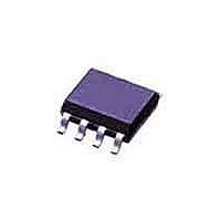
TISP6NTP2AD-S Bourns Inc., TISP6NTP2AD-S Datasheet - Page 2

TISP6NTP2AD-S
Manufacturer Part Number
TISP6NTP2AD-S
Description
Sidacs Quad Buffered PGate Forward Conducting
Manufacturer
Bourns Inc.
Datasheet
1.TISP6NTP2ADR-S.pdf
(7 pages)
Specifications of TISP6NTP2AD-S
Breakover Current Ibo Max
7 A
Rated Repetitive Off-state Voltage Vdrm
100 V
Off-state Leakage Current @ Vdrm Idrm
0.005 mA
Mounting Style
SMD/SMT
Package / Case
SO-8
Lead Free Status / RoHS Status
Lead free / RoHS Compliant
These systems often have the need to source two POTS (Plain Old Telephone Service) lines, one for a telephone and the other for a facsimile
machine. In a single surface mount package, the TISP6NTP2A protects the two POTS line SLICs (Subscriber Line Interface Circuits) against
overvoltages caused by lightning, a.c. power contact and induction.
The TISP6NTP2A has an array of four buffered P-gate forward conducting thyristors with twin commoned gates and a common anode
connection. Each thyristor cathode has a separate terminal connection. An antiparallel anode-cathode diode is connected across each
thyristor. The buffer transistors reduce the gate supply current.
In use, the cathodes of an TISP6NTP2A thyristor are connected to the four conductors of two POTS lines (see applications information). Each
gate is connected to the appropriate negative voltage battery feed of the SLIC driving that line pair. By having separate gates, each SLIC can
be protected at a voltage level related to the negative supply voltage of that individual SLIC. The anode of the TISP6NTP2A is connected to the
SLIC common.
Positive overvoltages are clipped to common by forward conduction of the TISP6NTP2A antiparallel diode. Negative overvoltages are initially
clipped close to the SLIC negative supply by emitter follower action of the TISP6NTP2A buffer transistor. If sufficient clipping current flows, the
TISP6NTP2A thyristor will regenerate and switch into a low voltage on-state condition. As the overvoltage subsides, the high holding current of
the TISP6NTP2A prevents d.c. latchup.
Description (continued)
Absolute Maximum Ratings, T A = 25
Repetitive peak off-state voltage, I
Repetitive peak gate-cathode voltage, V
Non-repetitive peak on-state pulse current, -40 °C ≤ T
Non-repetitive peak on-state current, 50/60 Hz, -40 °C ≤ T
Non-repetitive peak gate current, 1/2 µs pulse, cathodes commoned (see Note 1)
Operating free-air temperature range
Junction temperature
Storage temperature range
NOTES: 1. Initially, the protector must be in thermal equilibrium with -40 °C ≤ T
TISP6NTP2A Programmable Protector
10/1000 µs (Bellcore GR-1089-CORE, Issue 1, November 1994, Section 4)
0.2/310 µs (I3124, open-circuit voltage wave shape 0.5/700 µs)
5/310 µs (ITU-T K.20 & K.21, open-circuit voltage wave shape 10/700 µs)
8/20 µs (IEC 61000-4-5:1995, open-circuit voltage wave shape 1.2/50 µs)
2/10 µs (Bellcore GR-1089-CORE, Issue 1, November 1994, Section 4)
100 ms
1 s
5 s
300 s
900 s
2. These non-repetitive rated currents are peak values for either polarity. The rated current values may be applied to any cathode-
to its initial conditions.
anode terminal pair. Additionally, all cathode-anode terminal pairs may have their rated current values applied simultaneously (in
this case the anode terminal current will be four times the rated current value of an individual terminal pair). Above 85 °C, derate
linearly to zero at 150 °C lead temperature.
G
= 0, - 40 °C ≤ T
KA
°
C (Unless Otherwise Noted)
= 0, - 40 °C ≤ T
Rating
J
≤ 85 °C
J
≤ 85 °C, (see Notes 1 and 2)
J
J
≤ 85 °C
≤ 85 °C, (see Notes 1 and 2)
Customers should verify actual device performance in their specific applications.
J
≤ 85 °C. The surge may be repeated after the device returns
Specifications are subject to change without notice.
Symbol
V
V
I
I
GKRM
I
GSM
T
TSM
DRM
TSP
T
T
stg
A
J
-40 to +150
-65 to +150
JUNE 1998 - REVISED JULY 2008
-40 to +85
Value
-100
0.45
0.43
-90
2.7
1.5
20
25
25
75
85
25
7
Unit
°C
°C
°C
V
V
A
A
A


