82CNQ030APBF Vishay, 82CNQ030APBF Datasheet - Page 2
82CNQ030APBF
Manufacturer Part Number
82CNQ030APBF
Description
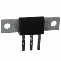
DIODE SCHOTTKY 30V 40A D61-8
Manufacturer
Vishay
Specifications of 82CNQ030APBF
Diode Configuration
1 Pair Common Cathode
Diode Type
Schottky
Voltage - Forward (vf) (max) @ If
550mV @ 80A
Current - Reverse Leakage @ Vr
5mA @ 30V
Current - Average Rectified (io) (per Diode)
40A
Voltage - Dc Reverse (vr) (max)
30V
Speed
Fast Recovery =< 500ns, > 200mA (Io)
Mounting Type
Through Hole, Radial
Package / Case
D-61-8
Product
Schottky Diodes
Peak Reverse Voltage
30 V
Forward Continuous Current
80 A
Max Surge Current
5100 A
Configuration
Dual Common Cathode
Forward Voltage Drop
0.55 V
Maximum Reverse Leakage Current
5000 uA
Operating Temperature Range
- 55 C to + 150 C
Mounting Style
Screw
Repetitive Reverse Voltage Vrrm Max
30V
Forward Current If(av)
80A
Forward Voltage Vf Max
550mV
Lead Free Status / RoHS Status
Lead free / RoHS Compliant
Reverse Recovery Time (trr)
-
Lead Free Status / Rohs Status
Lead free / RoHS Compliant
Other names
*82CNQ030APBF
VS-82CNQ030APBF
VS-82CNQ030APBF
VS82CNQ030APBF
VS82CNQ030APBF
VS-82CNQ030APBF
VS-82CNQ030APBF
VS82CNQ030APBF
VS82CNQ030APBF
Available stocks
Company
Part Number
Manufacturer
Quantity
Price

Part Number:
82CNQ030APBF
Manufacturer:
IR
Quantity:
20 000


VS-82CNQ030A PbF Series
Vishay High Power Products
Note
(1)
www.vishay.com
2
ABSOLUTE MAXIMUM RATINGS
PARAMETER
Maximum average forward current
See fig. 5
Maximum peak one cycle
non-repetitive surge current per leg
See fig. 7
Non-repetitive avalanche energy per leg
Repetitive avalanche current per leg
ELECTRICAL SPECIFICATIONS
PARAMETER
Maximum forward voltage drop per leg
See fig. 1
Maximum reverse leakage current per leg
See fig. 2
Maximum junction capacitance per leg
Typical series inductance per leg
Maximum voltage rate of change
THERMAL - MECHANICAL SPECIFICATIONS
PARAMETER
Maximum junction and storage
temperature range
Maximum thermal resistance,
junction to case
Typical thermal resistance,
case to heatsink
Approximate weight
Mounting torque
Marking device
Pulse width < 300 μs, duty cycle < 2 %
per package
maximum
minimum
per leg
For technical questions, contact:
SYMBOL
SYMBOL
SYMBOL
T
V
I
dV/dt
R
R
New Generation 3 D-61 Package, 2 x 40 A
J
I
RM
I
F(AV)
E
FM
, T
FSM
I
C
L
thJC
thCS
AR
AS
S
T
(1)
Stg
(1)
50 % duty cycle at T
5 μs sine or 3 μs rect. pulse
10 ms sine or 6 ms rect. pulse
T
Current decaying linearly to zero in 1 μs
Frequency limited by T
40 A
80 A
40 A
80 A
T
T
V
Measured lead to lead 5 mm from package body
Rated V
DC operation (see fig. 4)
DC operation
Mounting surface, smooth and greased
Device flatness < 5 mils
Case style D-61
Case style D-61-8-SM
Case style D-61-8-SL
J
J
J
R
= 25 °C, I
= 25 °C
= 125 °C
= 5 V
R
Schottky Rectifier
DC
(test signal range 100 kHz to 1 MHz), 25 °C
AS
diodestech@vishay.com
= 8 A, L = 1.12 mH
TEST CONDITIONS
TEST CONDITIONS
TEST CONDITIONS
C
= 119 °C, rectangular waveform
J
maximum V
T
T
V
J
J
R
= 25 °C
= 125 °C
Following any rated
load condition and with
rated V
= Rated V
A
= 1.5 x V
RRM
R
applied
R
typical
Document Number: 94258
- 55 to 150
VALUES
VALUES
VALUES
10 000
40 (35)
58 (50)
5100
3700
0.47
0.55
0.37
0.47
82CNQ030ASM
Revision: 16-Apr-10
880
280
82CNQ030ASL
0.85
0.42
0.30
0.28
5.5
80
36
7.8
8
5
82CNQ030A
kgf · cm
UNITS
UNITS
(lbf · in)
UNITS
V/μs
°C/W
mA
mJ
nH
pF
oz.
A
A
°C
V
g
Related parts for 82CNQ030APBF
Image
Part Number
Description
Manufacturer
Datasheet
Request
R

Part Number:
Description:
DIODE SCHOTTKY 30V 40A D61-8
Manufacturer:
Vishay
Datasheet:

Part Number:
Description:
357-036-542-201 CARDEDGE 36POS DL .156 BLK LOPRO
Manufacturer:
Vishay
Datasheet:
Part Number:
Description:
357-036-542-201 CARDEDGE 36POS DL .156 BLK LOPRO
Manufacturer:
Vishay
Datasheet:
Part Number:
Description:
357-036-542-201 CARDEDGE 36POS DL .156 BLK LOPRO
Manufacturer:
Vishay
Datasheet:
Part Number:
Description:
357-036-542-201 CARDEDGE 36POS DL .156 BLK LOPRO
Manufacturer:
Vishay
Datasheet:
Part Number:
Description:
357-036-542-201 CARDEDGE 36POS DL .156 BLK LOPRO
Manufacturer:
Vishay
Datasheet:
Part Number:
Description:
357-036-542-201 CARDEDGE 36POS DL .156 BLK LOPRO
Manufacturer:
Vishay
Datasheet:
Part Number:
Description:
357-036-542-201 CARDEDGE 36POS DL .156 BLK LOPRO
Manufacturer:
Vishay
Datasheet:
Part Number:
Description:
357-036-542-201 CARDEDGE 36POS DL .156 BLK LOPRO
Manufacturer:
Vishay
Datasheet:
Part Number:
Description:
357-036-542-201 CARDEDGE 36POS DL .156 BLK LOPRO
Manufacturer:
Vishay
Datasheet:
Part Number:
Description:
357-036-542-201 CARDEDGE 36POS DL .156 BLK LOPRO
Manufacturer:
Vishay
Datasheet:
Part Number:
Description:
357-036-542-201 CARDEDGE 36POS DL .156 BLK LOPRO
Manufacturer:
Vishay
Datasheet:
Part Number:
Description:
357-036-542-201 CARDEDGE 36POS DL .156 BLK LOPRO
Manufacturer:
Vishay
Datasheet:
Part Number:
Description:
357-036-542-201 CARDEDGE 36POS DL .156 BLK LOPRO
Manufacturer:
Vishay
Datasheet:
Part Number:
Description:
357-036-542-201 CARDEDGE 36POS DL .156 BLK LOPRO
Manufacturer:
Vishay
Datasheet: