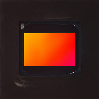
MT9V022IA7ATC Aptina LLC, MT9V022IA7ATC Datasheet - Page 7

MT9V022IA7ATC
Manufacturer Part Number
MT9V022IA7ATC
Description
SENSOR IMAGE VGA COLOR 52IBGA
Manufacturer
Aptina LLC
Type
CMOS Imagingr
Series
DigitalClarity®r
Specifications of MT9V022IA7ATC
Pixel Size
6µm x 6µm
Active Pixel Array
752H x 480V
Frames Per Second
60
Voltage - Supply
3.3V
Package / Case
52-IBGA
Sensor Image Color Type
Color
Sensor Image Size Range
250,920 to 480,000Pixels
Sensor Image Size
752x480Pixels
Operating Supply Voltage (min)
3V
Operating Supply Voltage (typ)
3.3V
Operating Supply Voltage (max)
3.6V
Operating Temp Range
-40C to 85C
Package Type
IBGA
Operating Temperature Classification
Industrial
Mounting
Surface Mount
Pin Count
52
Lead Free Status / RoHS Status
Lead free / RoHS Compliant
Other names
557-1166
Available stocks
Company
Part Number
Manufacturer
Quantity
Price
Company:
Part Number:
MT9V022IA7ATC
Manufacturer:
ATMEL
Quantity:
3 060
Part Number:
MT9V022IA7ATC
Manufacturer:
MICRON/美光
Quantity:
20 000
Part Number:
MT9V022IA7ATC ES
Manufacturer:
MICRON/美光
Quantity:
20 000
Part Number:
MT9V022IA7ATC QS
Manufacturer:
MICRON/美光
Quantity:
20 000
Automatic Gain Control (AGC) and Automatic Exposure Control (AEC)
Pixel Clock Speed
Gain Settings
Analog Gain
Digital Gain
Figure 9:
Read Mode Options
Column and Row Flip
PDF:09005aef8201ffc3/Source: 09005aef81ff2525
MT9V022_Product_Brief - Rev. A 1/06 EN
Digital Gain Tiled Sample
The integrated AEC/AGC unit is responsible for ensuring that optimal auto settings of
exposure and (analog) gain are computed and updated every frame.
When the AGC or AEC are enabled, the MT9V022 measures current scene luminosity
and desired output luminosity by accumulating a histogram of pixel values while read-
ing out a frame. The desired exposure and gain are then calculated and applied for the
subsequent frame.
The pixel clock speed is same as the master clock of 26.66 MHz by default. However,
when column binning 2 or 4 is enabled, the pixel clock speed will be reduced by half or
one-fourth of the master clock speed, respectively.
The analog gain range supported in the MT9V022 is 1X–4X with a step size of 6.25
percent.
In the MT9V022, the user either may apply a single gain value for the entire array or they
may divide the image into 25 tiles (Figure 9) through the two-wire serial interface and
apply digital gain individually to each tile.
The coordinates and digital gain (0.25 - 3.75X) of each tile may be individually pro-
grammed via the two-wire serial interface. This feature should help improve pulling
detail out of regions of an image that are either dark, or lighter than the rest of the scene
without affecting the rest of the scene.
To ease mounting orientation issues, the MT9V022 column and row readout order can
be independently reversed via the two-wire serial interface. The image will then be rep-
resented correctly regardless of camera orientation.
Y
Y
Y
Y
Y
Y
0/5
1/5
2/5
3/5
4/5
5/5
X
0/5
x0_y0
x0_y1
x0_y2
x0_y3
x0_y4
X
1/5
x1_y0
x1_y1
x1_y2
x1_y3
x1_y4
X
2/5
MT9V022: 1/3-Inch Wide-VGA Digital Image Sensor
X
3/5
7
X
5/5
Micron Technology, Inc., reserves the right to change products or specifications without notice.
x4_y0
x4_y1
x4_y2
x4_y3
x4_y4
X
5/5
Output Data Timing
©2006 Micron Technology, Inc. All rights reserved.


