MT9M001C12STM Aptina LLC, MT9M001C12STM Datasheet - Page 14
MT9M001C12STM
Manufacturer Part Number
MT9M001C12STM
Description
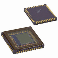
SENSOR IMAGE MONO CMOS 48-LCC
Manufacturer
Aptina LLC
Type
CMOS Imagingr
Datasheets
1.MT9M001C12STM.pdf
(35 pages)
2.MT9M001C12STM.pdf
(2 pages)
3.MT9M001C12STM.pdf
(28 pages)
Specifications of MT9M001C12STM
Pixel Size
5.2µm x 5.2µm
Active Pixel Array
1280H x 1024V
Frames Per Second
30
Voltage - Supply
3 V ~ 3.6 V
Package / Case
48-CLCC
Sensor Image Color Type
Monochrome
Sensor Image Size
1280x1024Pixels
Operating Supply Voltage (min)
3V
Operating Supply Voltage (typ)
3.3V
Operating Supply Voltage (max)
3.6V
Operating Temp Range
0C to 70C
Package Type
CLCC
Operating Temperature Classification
Commercial
Mounting
Surface Mount
Pin Count
48
Lead Free Status / RoHS Status
Lead free / RoHS Compliant
Other names
557-1151
Q3930625
Q3990821
Q3930625
Q3990821
Available stocks
Company
Part Number
Manufacturer
Quantity
Price
Company:

Part Number:
MT9M001C12STM
Manufacturer:
MICRON
Quantity:
1 000
Part Number:
MT9M001C12STM
Manufacturer:
MICRON/镁光
Quantity:
20 000


Two-Wire Serial Interface Sample Write and Read Sequences
16-Bit Write Sequence
Figure 8:
16-Bit Read Sequence
Figure 9:
PDF:7657919000/Source: 7657919000
MT9M001_DS - Rev. J 5/10 EN
S
SCLK
DATA
S
SCLK
DATA
START
START
0xBA ADDR
Timing Diagram Showing a Write to Reg0x09 with the Value 0x0284
Timing Diagram Showing a Read from Reg0x09; Returned Value 0x0284
0xBA ADDR
ACK
A typical write sequence for writing 16 bits to a register is shown in Figure 8. A start bit
given by the master, followed by the write address, starts the sequence. The image sensor
will then give an acknowledge bit and expects the register address to come first, followed
by the 16-bit data. After each eight-bit transfer, the image sensor will give an acknowl-
edge bit. All 16 bits must be written before the register will be updated. After 16 bits are
transferred, the register address is automatically incremented so that the next 16 bits are
written to the next register. The master stops writing by sending a start or stop bit.
A typical read sequence is shown in Figure 9. First the master has to write the register
address, as in a write sequence. Then a start bit and the read address specifies that a read
is about to happen from the register. The master then clocks out the register data eight
bits at a time. The master sends an acknowledge bit after each eight-bit transfer. The
register address should be incremented after every 16 bits is transferred. The data
transfer is stopped when the master sends a no-acknowledge bit.
ACK
Reg0x09
Reg0x09
ACK
Two-Wire Serial Interface Sample Write and Read Sequences
0xBB ADDR
ACK
14
MT9M001: 1/2-Inch Megapixel Digital Image Sensor
0000 0010
ACK
0000 0010
ACK
Aptina reserves the right to change products or specifications without notice.
ACK
1000 0100
©2004 Aptina Imaging Corporation. All rights reserved.
1000 0100
ACK
NACK
STOP
STOP
Related parts for MT9M001C12STM
Image
Part Number
Description
Manufacturer
Datasheet
Request
R

Part Number:
Description:
SENSOR IMAGE VGA COLOR CMOS PLCC
Manufacturer:
Aptina LLC
Datasheet:

Part Number:
Description:
IC SENSOR IMAGE COLOR 48CLCC
Manufacturer:
Aptina LLC
Datasheet:

Part Number:
Description:
SENSOR IMAGE 1.3MP CMOS 48-CLCC
Manufacturer:
Aptina LLC
Datasheet:

Part Number:
Description:
SENSOR IMAGE 2MP CMOS 48-CLCC
Manufacturer:
Aptina LLC
Datasheet:

Part Number:
Description:
SENSOR IMAGE VGA MONO 52IBGA
Manufacturer:
Aptina LLC
Datasheet:

Part Number:
Description:
SENSOR IMAGE VGA COLOR 48CLCC
Manufacturer:
Aptina LLC
Datasheet:

Part Number:
Description:
SENSOR IMAGE COLOR CMOS 48-PLCC
Manufacturer:
Aptina LLC
Datasheet:

Part Number:
Description:
KIT HEAD BOARD FOR MT9P031
Manufacturer:
Aptina LLC
Datasheet:

Part Number:
Description:
KIT HEAD BOARD FOR MT9D131
Manufacturer:
Aptina LLC
Datasheet:

Part Number:
Description:
KIT HEAD BOARD FOR MT9P031
Manufacturer:
Aptina LLC
Datasheet:
Part Number:
Description:
SENSOR IMAGE VGA COLOR CMOS PLCC
Manufacturer:
Aptina LLC
Datasheet:
Part Number:
Description:
IC SENSOR IMAGE COLOR 48CLCC
Manufacturer:
Aptina LLC
Datasheet:
Part Number:
Description:
SENSOR IMAGE 2MP CMOS 48-CLCC
Manufacturer:
Aptina LLC
Datasheet:
