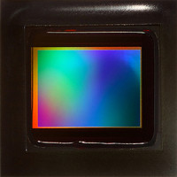
MT9P031I12STM Aptina LLC, MT9P031I12STM Datasheet - Page 6

MT9P031I12STM
Manufacturer Part Number
MT9P031I12STM
Description
SENSOR IMAGE 5MP MONO CMOS 48LCC
Manufacturer
Aptina LLC
Type
CMOS Imagingr
Datasheets
1.MT9P031I12STCH_ES.pdf
(12 pages)
2.MT9P031I12STCH_ES.pdf
(2 pages)
3.MT9P031I12STM.pdf
(12 pages)
Specifications of MT9P031I12STM
Package / Case
48-iLCC
Pixel Size
2.2µm x 2.2µm
Active Pixel Array
2592H x 1944V
Frames Per Second
60
Voltage - Supply
2.6 V ~ 3.1 V
Supply Voltage Range
1.7V To 3.1V, 1.7V To 1.9V, 2.6V To 3.1V
Operating Temperature Range
-30°C To +70°C
Digital Ic Case Style
PLCC
No. Of Pins
48
Supply Voltage Max
3.1V
Ic Function
Digital Image Sensor
Rohs Compliant
Yes
Lead Free Status / RoHS Status
Lead free / RoHS Compliant
For Use With
557-1430 - KIT HEAD BOARD FOR MT9P031557-1429 - KIT DEV FOR MT9P031
Lead Free Status / RoHS Status
Lead free / RoHS Compliant, Lead free / RoHS Compliant
Other names
557-1397
Q3884047
Q3956538
Q4007187
Q3884047
Q3956538
Q4007187
Available stocks
Company
Part Number
Manufacturer
Quantity
Price
Company:
Part Number:
MT9P031I12STM
Manufacturer:
ADI
Quantity:
119
Part Number:
MT9P031I12STM
Manufacturer:
APTINA
Quantity:
20 000
Company:
Part Number:
MT9P031I12STM-DP
Manufacturer:
ON
Quantity:
210
Company:
Part Number:
MT9P031I12STMD ES
Manufacturer:
Aptina LLC
Quantity:
135
Table 2:
PDF: 09005aef824c993e/Source: 09005aef824c9943
MT9P031_5100_PB_2.fm - Rev. B 8/07 EN
FRAME_VALID
LINE_VALID
STANDBY#
D
TRIGGER
EXTCLK
OUT
STROBE
VAAPIX
RESET#
PIXCLK
V
Name
S
S
V
RSVD
D
A
SCLK
TEST
DD
OE#
ADDR
V
V
DATA
NC
DD
GND
GND
DD
AA
[11:0]
PLL
Q
Pin Descriptions
18, 19, 27, 28, 29,
LLCC Pin
10, 26, 46
3, 20, 21
33 to 45
11, 39
23, 24
12, 7
1, 48
2, 22
16
31
17
14
15
13
32
25
30
4
5
7
8
9
6
Output
Output
Output
Output
Output
Supply
Supply
Supply
Supply
Supply
Supply
Supply
Input
Input
Input
Input
Input
Input
Input
Type
I/O
–
–
–
When LOW, the MT9P031 asynchronously resets. When driven HIGH, it
resumes normal operation with all configuration registers set to factory
defaults.
External input clock.
Serial clock: Pull to V
When HIGH, the PIXCLK, D
outputs enter a High-Z. When driven LOW, normal operation resumes.
Standby: When LOW, the chip enters a low-power standby mode. It
resumes normal operation when the pin is driven HIGH.
Snapshot trigger: Used to trigger one frame of output in snapshot
modes and to indicate the end of exposure in bulb exposure modes.
Serial address: When HIGH, the MT9P031 responds to device ID (BA)
When LOW, it responds to serial device ID (90)
Serial data: Pull to V
Pixel clock: The D
outputs should be captured on the falling edge of this signal.
Pixel data: Pixel data is 12-bit. MSB (D
each pixel, to be captured on the falling edge of PIXCLK.
Frame valid: Driven HIGH during active pixels and horizontal blanking
of each frame and LOW during vertical blanking.
Line valid: Driven HIGH with active pixels of each line and LOW during
blanking periods.
Snapshot strobe: Driven HIGH when all pixels are exposing in
snapshot modes.
Digital supply voltage: Nominally 1.8V.
IO supply voltage: Nominally 1.8V or 2.8V.
Digital ground.
Analog supply voltage: Nominally 2.8V.
Pixel supply voltage: Nominally 2.8V, connected externally to V
Analog ground.
PLL supply voltage: Nominally 2.8V, connected externally to V
Tie to A
Tie to D
No connect.
MT9P031: 1/2.5-Inch 5-Mp Digital Image Sensor
GND
GND
6
for normal device operation (factory use only).
for normal device operation (factory use only).
OUT
Micron Technology, Inc., reserves the right to change products or specifications without notice.
DD
DD
, FRAME_VALID, LINE_VALID, and STROBE
Q with a 1.5
Q with a 1.5
OUT
Description
, FRAME_VALID, LINE_VALID, and STROBE
KΩ
KΩ
OUT
resistor.
resistor.
11) through LSB (D
Functional Overview
©2006 Micron Technology, Inc. All rights reserved.
H
.
OUT
AA
0) of
AA
.
.
H
.


