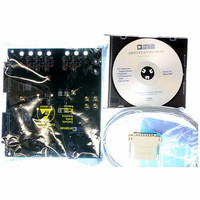
AD9743-EBZ Analog Devices Inc, AD9743-EBZ Datasheet - Page 12
AD9743-EBZ
Manufacturer Part Number
AD9743-EBZ
Description
BOARD EVALUATION 10BIT AD9743
Manufacturer
Analog Devices Inc
Series
TxDAC®r
Datasheet
1.AD9743-EBZ.pdf
(28 pages)
Specifications of AD9743-EBZ
Number Of Dac's
2
Number Of Bits
10
Outputs And Type
2, Differential
Sampling Rate (per Second)
250M
Data Interface
Serial, Parallel
Dac Type
Current
Voltage Supply Source
Analog and Digital
Operating Temperature
-40°C ~ 85°C
Utilized Ic / Part
AD9743
Lead Free Status / RoHS Status
Lead free / RoHS Compliant
Settling Time
-
Lead Free Status / RoHS Status
Compliant, Lead free / RoHS Compliant


AD9741/AD9743/AD9745/AD9746/AD9747
Table 11. AD9746 Pin Function Descriptions
Pin No.
1, 6
2, 5
3
4
7, 28, 48
8, 47
9 to 22
23, 24, 26, 30, 45, 46
25
27
29
31 to 44
49
50
51
52
53
54
55
56, 57, 71, 72
58, 61, 64, 67, 70
59
60
62
63
65
66
68
69
EPAD
SDIO
SCLK
CSB
FSADJ
REFIO
Mnemonic
CVDD18
CVSS
CLKP
CLKN
DVSS
DVDD18
P1D<13:0>
NC
DCO
DVDD33
IQSEL
P2D<13:0>
SDO
RESET
AVDD33
AVSS
IOUT2P
IOUT2N
AUX2P
AUX2N
AUX1N
AUX1P
IOUT1N
IOUT1P
AVSS
NC = NO CONNECT
Description
Clock Supply Voltage (1.8 V).
Clock Supply Common (0 V).
Differential DAC Clock Input.
Complementary Differential DAC Clock Input.
Digital Supply Common (0 V).
Digital Core Supply Voltage (1.8 V).
Port 1 Data Bit Inputs.
No Connect.
Data Clock Output. Use to clock data source.
Digital I/O Supply Voltage (3.3 V).
I/Q Framing Signal for Single-Port Mode Operation.
Port 2 Data Bit Inputs.
Serial Peripheral Interface Data Output.
Serial Peripheral Interface Data Input and Optional Data Output.
Serial Peripheral Interface Clock Input.
Serial Peripheral Interface Chip Select Input. Active low.
Hardware Reset. Active high.
Full-Scale Current Output Adjust. Connect a 10 kΩ resistor to AVSS.
Reference Input/Output. Connect a 0.1 μF capacitor to AVSS.
Analog Supply Voltage (3.3 V).
Analog Supply Common (0 V).
DAC2 Current Output True. Sources full-scale current when input data bits are all 1.
DAC2 Current Output Complement. Sources full-scale current when data bits are all 0.
Auxiliary DAC2 Default Current Output Pin.
Auxiliary DAC2 Optional Output Pin. Enable through SPI.
Auxiliary DAC1 Optional Output Pin. Enable through SPI.
Auxiliary DAC1 Default Current Output Pin.
Complementary DAC1 Current Output. Sources full-scale current when data bits are all 0.
DAC1 Current Output. Sources full-scale current when data bits are all 1.
Exposed Thermal Pad. Must be soldered to copper pour on top surface of PCB for mechanical stability
and must be electrically tied to low impedance GND plane for low noise performance.
CVDD18
CVDD18
DVDD18
P1D13
P1D12
P1D10
P1D11
CLKN
CVSS
CLKP
CVSS
DVSS
P1D9
P1D8
P1D7
P1D6
P1D5
P1D4
10
11
12
13
14
15
16
17
18
1
2
3
4
5
6
7
8
9
Figure 5. AD9746 Pin Configuration
PIN 1
INDICATOR
Rev. 0 | Page 12 of 28
(TOP VIEW)
AD9746
54
53
52
51
50
49
48
47
46
45
44
43
42
41
40
39
38
37
FSADJ
RESET
CSB
SCLK
SDIO
SDO
DVSS
DVDD18
NC
NC
P2D0
P2D1
P2D2
P2D3
P2D4
P2D5
P2D6
P2D7
Related parts for AD9743-EBZ
Image
Part Number
Description
Manufacturer
Datasheet
Request
R

Part Number:
Description:
Dual 10Bit, 200 MSPS D-A Converter
Manufacturer:
Analog Devices Inc
Datasheet:

Part Number:
Description:
±1.7g Dual-Axis IMEMS Accelerometer Evaluation Board
Manufacturer:
Analog Devices Inc
Datasheet:
Part Number:
Description:
Inertial Sensor Evaluation System
Manufacturer:
Analog Devices Inc
Datasheet:
Part Number:
Description:
Manufacturer:
Analog Devices Inc
Datasheet:
Part Number:
Description:
Manufacturer:
Analog Devices Inc
Datasheet:
Part Number:
Description:
Manufacturer:
Analog Devices Inc
Datasheet:
Part Number:
Description:
Manufacturer:
Analog Devices Inc
Datasheet:
Part Number:
Description:
Manufacturer:
Analog Devices Inc
Datasheet:
Part Number:
Description:
Manufacturer:
Analog Devices Inc
Datasheet:
Part Number:
Description:
Manufacturer:
Analog Devices Inc
Datasheet:
Part Number:
Description:
Manufacturer:
Analog Devices Inc
Datasheet:
Part Number:
Description:
Manufacturer:
Analog Devices Inc
Datasheet:
Part Number:
Description:
Manufacturer:
Analog Devices Inc
Datasheet: