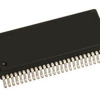
MM908E625ACDWB Freescale Semiconductor, MM908E625ACDWB Datasheet - Page 34

MM908E625ACDWB
Manufacturer Part Number
MM908E625ACDWB
Description
IC QUAD HALF BRDG MCU/LIN 54SOIC
Manufacturer
Freescale Semiconductor
Datasheets
1.MM908E625.pdf
(48 pages)
2.MM908E625ACDWB.pdf
(48 pages)
3.MM908E625ACDWB.pdf
(48 pages)
4.MM908E625ACDWB.pdf
(48 pages)
5.MM908E625ACDWB.pdf
(40 pages)
Specifications of MM908E625ACDWB
Applications
Automotive Mirror Control
Core Processor
HC08
Program Memory Type
FLASH (16 kB)
Controller Series
908E
Ram Size
512 x 8
Interface
SCI, SPI
Number Of I /o
13
Voltage - Supply
8 V ~ 18 V
Operating Temperature
-40°C ~ 85°C
Mounting Type
Surface Mount
Package / Case
54-SOIC (0.300", 7.50mm Width) Exposed Pad
Program Memory Size
16 KB
Number Of Programmable I/os
54
Number Of Timers
16
Operating Supply Voltage
- 18 V to + 28 V
Maximum Operating Temperature
+ 85 C
Mounting Style
SMD/SMT
Minimum Operating Temperature
- 40 C
Lead Free Status / RoHS Status
Contains lead / RoHS non-compliant
Available stocks
Company
Part Number
Manufacturer
Quantity
Price
Company:
Part Number:
MM908E625ACDWB
Manufacturer:
FREESCALE Semiconductor
Quantity:
26
Switchable VDD Outputs
can be used for driving external circuitry that requires a V
voltage. The output is enabled with bit PSON in the System
Control Register and can be switched on/off with bit HVDDON
in the Power Output Register. Low- or high-voltage conditions
(LVI/HVI) have no influence on this circuitry.
HVDD Overtemperature Protection
temperature reset is enabled.
HVDD Overcurrent Protection
event the overcurrent limit is or was reached, the output
automatically switches off and the HVDD overcurrent flag in the
System Status Register is set.
908E625
34
The HVDD terminal is a switchable VDD output terminal. It
Overtemperature protection is enabled if the high-
The HVDD output is protected against overcurrent. In the
HS Current
FGEN Input
(MCU PWM
Signal)
HS Overcurrent Shutdown Threshold
Figure 20. Inrush Current Limiter on High-Side Output
Freescale Semiconductor, Inc.
For More Information On This Product,
Go to: www.freescale.com
DD
System Control Register (SYSCTL)
PSON—Power Stages On Bit
high side, LIN transmitter, Analog Input PA1 current sources,
and HVDD output). Reset clears the PSON bit.
Reset
Read
Write
This read/write bit enables the power stages (half-bridges,
• 1 = Power stages enabled.
• 0 = Power stages disabled.
MOTOROLA ANALOG INTEGRATED CIRCUIT DEVICE DATA
PSON
Bit7
0
Register Name and Address: SYSCTL - $03
SRS1
6
0
SRS0
5
0
4
0
0
3
0
0
2
0
0
1
0
0
Bit0
t
t
GS
0
0


