DSPIC33FJ32GS606-I/MR Microchip Technology, DSPIC33FJ32GS606-I/MR Datasheet - Page 315
DSPIC33FJ32GS606-I/MR
Manufacturer Part Number
DSPIC33FJ32GS606-I/MR
Description
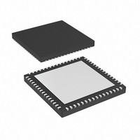
16 Bit MCU/DSP 40MIPS 32KB FLASH 64 QFN 9x9x0.9mm TUBE
Manufacturer
Microchip Technology
Series
dsPIC™ 33Fr
Specifications of DSPIC33FJ32GS606-I/MR
Core Processor
dsPIC
Core Size
16-Bit
Speed
40 MIPs
Connectivity
I²C, IrDA, LIN, SPI, UART/USART
Peripherals
Brown-out Detect/Reset, QEI, POR, PWM, WDT
Number Of I /o
58
Program Memory Size
32KB (32K x 8)
Program Memory Type
FLASH
Ram Size
4K x 8
Voltage - Supply (vcc/vdd)
3 V ~ 3.6 V
Data Converters
A/D 16x10b; D/A 1x10b
Oscillator Type
Internal
Operating Temperature
-40°C ~ 85°C
Package / Case
64-VFQFN, Exposed Pad
Lead Free Status / RoHS Status
Lead free / RoHS Compliant
Eeprom Size
-
Lead Free Status / RoHS Status
Lead free / RoHS Compliant


REGISTER 22-4:
REGISTER 22-5:
2010 Microchip Technology Inc.
bit 15
bit 7
Legend:
R = Readable bit
-n = Value at POR
bit 15-0
bit 15
bit 7
Legend:
R = Readable bit
-n = Value at POR
bit 15-8
bit 7-0
Note:
Note:
dsPIC33FJ32GS406/606/608/610 and dsPIC33FJ64GS406/606/608/610
PCFG15
PCFG23
PCFG7
R/W-0
R/W-0
R/W-0
U-0
—
Not all PCFGx bits are available on all devices. See Figure 22-1, Figure 22-2, Figure 22-3, and Figure 22-4
for the available analog inputs (PCFGx = ANx, where x = 0-15).
Not all PCFGx bits are available on all devices. See Figure 22-1, Figure 22-2, Figure 22-3, and Figure 22-4
for the available analog inputs (PCFGx = ANx, where x can be 0 through 15).
PCFG<15:0>: A/D Port Configuration Control bits
1 = Port pin in Digital mode, port read input enabled, A/D input multiplexor connected to AV
0 = Port pin in Analog mode, port read input disabled, A/D samples pin voltage
Unimplemented: Read as ‘0’
PCFG<23:16>: A/D Port Configuration Control bits
1 = Port pin in Digital mode, port read input enabled, A/D input multiplexor connected to AV
0 = Port pin in Analog mode, port read input disabled, A/D samples pin voltage
PCFG14
PCFG22
PCFG6
R/W-0
R/W-0
R/W-0
U-0
—
ADPCFG: A/D PORT CONFIGURATION REGISTER
ADPCFG2: A/D PORT CONFIGURATION REGISTER
W = Writable bit
‘1’ = Bit is set
W = Writable bit
‘1’ = Bit is set
PCFG13
PCFG21
PCFG5
R/W-0
R/W-0
R/W-0
U-0
—
PCFG12
PCFG20
PCFG4
R/W-0
R/W-0
R/W-0
U-0
Preliminary
—
U = Unimplemented bit, read as ‘0’
U = Unimplemented bit, read as ‘0’
‘0’ = Bit is cleared
‘0’ = Bit is cleared
PCFG19
PCFG11
PCFG3
R/W-0
R/W-0
R/W-0
U-0
—
PCFG10
PCFG18
PCFG2
R/W-0
R/W-0
R/W-0
U-0
—
x = Bit is unknown
x = Bit is unknown
PCFG17
PCFG9
PCFG1
R/W-0
R/W-0
R/W-0
U-0
—
DS70591C-page 315
PCFG16
PCFG8
PCFG0
R/W-0
R/W-0
R/W-0
SS
SS
U-0
—
bit 8
bit 0
bit 8
bit 0
Related parts for DSPIC33FJ32GS606-I/MR
Image
Part Number
Description
Manufacturer
Datasheet
Request
R

Part Number:
Description:
IC, DSC, 16BIT, 12KB, 40MHZ, 3.6V, DIP28
Manufacturer:
Microchip Technology
Datasheet:

Part Number:
Description:
Manufacturer:
Microchip Technology Inc.
Datasheet:
Part Number:
Description:
Manufacturer:
Microchip Technology Inc.
Datasheet:
Part Number:
Description:
Manufacturer:
Microchip Technology Inc.
Datasheet:
Part Number:
Description:
Manufacturer:
Microchip Technology Inc.
Datasheet:
Part Number:
Description:
Manufacturer:
Microchip Technology Inc.
Datasheet:
Part Number:
Description:
Manufacturer:
Microchip Technology Inc.
Datasheet:
Part Number:
Description:
Manufacturer:
Microchip Technology Inc.
Datasheet:
Part Number:
Description:
Manufacturer:
Microchip Technology Inc.
Datasheet: