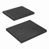
CY7C1370D-200BZI Cypress Semiconductor Corp, CY7C1370D-200BZI Datasheet - Page 19

CY7C1370D-200BZI
Manufacturer Part Number
CY7C1370D-200BZI
Description
IC,SYNC SRAM,512KX36,CMOS,BGA,165PIN,PLASTIC
Manufacturer
Cypress Semiconductor Corp
Datasheet
1.CY7C1372D-200AXC.pdf
(29 pages)
Specifications of CY7C1370D-200BZI
Format - Memory
RAM
Memory Type
SRAM - Synchronous
Memory Size
18M (512K x 36)
Speed
200MHz
Interface
Parallel
Voltage - Supply
3.135 V ~ 3.6 V
Operating Temperature
-40°C ~ 85°C
Package / Case
165-LFBGA
Lead Free Status / RoHS Status
Contains lead / RoHS compliant by exemption
Available stocks
Company
Part Number
Manufacturer
Quantity
Price
Company:
Part Number:
CY7C1370D-200BZI
Manufacturer:
Cypress Semiconductor Corp
Quantity:
10 000
Part Number:
CY7C1370D-200BZI
Manufacturer:
CYPRESS
Quantity:
20 000
Company:
Part Number:
CY7C1370D-200BZIT
Manufacturer:
Cypress Semiconductor Corp
Quantity:
10 000
Maximum Ratings
Exceeding maximum ratings may impair the useful life of the
device. These user guidelines are not tested.
Storage Temperature ................................. –65°C to +150°C
Ambient Temperature with
Power Applied ............................................ –55°C to +125°C
Supply Voltage on V
Supply Voltage on V
DC to Outputs in Tristate .....................–0.5V to V
DC Input Voltage ................................... –0.5V to V
Current into Outputs (LOW)......................................... 20 mA
Static Discharge Voltage.......................................... > 2001V
(per MIL-STD-883, Method 3015)
Latch up Current.................................................... > 200 mA
Operating Range
Electrical Characteristics
Over the Operating Range
Document Number: 38-05555 Rev. *K
Commercial
Industrial
V
V
V
V
V
V
I
I
I
I
Notes
X
OZ
DD
SB1
16. Overshoot: V
17. T
DD
DDQ
OH
OL
IH
IL
Parameter
Range
Power-up
: Assumes a linear ramp from 0V to V
–40°C to +85°C
IH
Temperature
0°C to +70°C 3.3V–5%/+10% 2.5V –5% to
Power Supply Voltage
I/O Supply Voltage
Output HIGH Voltage
Output LOW Voltage
Input HIGH Voltage
Input LOW Voltage
Input Leakage Current
except ZZ and MODE
Input Current of MODE
Input Current of ZZ
Output Leakage Current GND V
V
Automatic CE
Power-down
Current—TTL Inputs
(AC) < V
DD
Ambient
Operating Supply
DD
DDQ
Description
DD
Relative to GND ........–0.5V to +4.6V
Relative to GND ...... –0.5V to +V
+1.5V (Pulse width less than t
[16, 17]
[16]
[16]
V
DD
for 3.3V I/O
for 2.5V I/O
for 3.3V I/O, I
for 2.5V I/O, I
for 3.3V I/O, I
for 2.5V I/O, I
for 3.3V I/O
for 2.5V I/O
for 3.3V I/O
for 2.5V I/O
GND V
Input = V
Input = V
Input = V
Input = V
V
f = f
Max. V
V
DD
DD
(min.) within 200 ms. During this time V
IH
MAX
= Max., I
or V
DD
= 1/t
CYC
I
SS
DD
SS
DD
I
DDQ
, Device Deselected, V
IN
V
V
DD
V
/2), undershoot: V
V
V
CYC
DDQ
OH
OH
OL
OL
OUT
DDQ
DDQ,
DD
+ 0.5V
+ 0.5V
IL
= 8.0 mA
= 1.0 mA
= –4.0 mA
= –1.0 mA
, f = f
= 0 mA,
DD
Output Disabled
Test Conditions
MAX
= 1/t
IL
(AC)> –2V (Pulse width less than t
Neutron Soft Error Immunity
LSBU
LMBU
SEL
* No LMBU or SEL events occurred during testing; this column represents a
statistical
cation Note AN 54908 “Accelerated Neutron SER Testing and Calculation of
Terrestrial Failure Rates”
Parameter
CYC
IN
IH
4-ns cycle, 250 MHz
5-ns cycle, 200 MHz
6-ns cycle, 167 MHz
4-ns cycle, 250 MHz
5-ns cycle, 200 MHz
6-ns cycle, 167 MHz
< V
2
DD
, 95% confidence limit calculation. For more details refer to Appli-
and V
Single Event
Description
Single-Bit
Latch up
Multi-Bit
DDQ
Logical
Upsets
Logical
Upsets
<V
CY7C1370D, CY7C1372D
DD
CYC
.
/2).
Conditions
3.135
3.135
2.375
Min.
–0.3
–0.3
–30
2.4
2.0
2.0
1.7
–5
–5
–5
25°C
25°C
85°C
Test
V
V
DD
DD
2.625
Max.
V
350
300
275
160
150
140
Typ Max* Unit
361
3.6
0.4
0.4
0.8
0.7
30
+ 0.3V
+ 0.3V
DD
5
5
5
0
0
Page 19 of 29
0.01
394
0.1
Unit
mA
mA
mA
mA
mA
mA
A
A
A
A
A
A
V
V
V
V
V
V
V
V
V
V
V
FIT/
FIT/
FIT/
Dev
Mb
Mb
[+] Feedback


