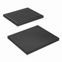
CY7C1315BV18-167BZC Cypress Semiconductor Corp, CY7C1315BV18-167BZC Datasheet - Page 7

CY7C1315BV18-167BZC
Manufacturer Part Number
CY7C1315BV18-167BZC
Description
SRAM (Static RAM)
Manufacturer
Cypress Semiconductor Corp
Datasheet
1.CY7C1313BV18-167BZC.pdf
(28 pages)
Specifications of CY7C1315BV18-167BZC
Format - Memory
RAM
Memory Type
SRAM - Synchronous, QDR II
Memory Size
18M (512K x 36)
Speed
167MHz
Interface
Parallel
Voltage - Supply
1.7 V ~ 1.9 V
Operating Temperature
0°C ~ 70°C
Package / Case
165-LFBGA
Lead Free Status / RoHS Status
Contains lead / RoHS non-compliant
Available stocks
Company
Part Number
Manufacturer
Quantity
Price
Company:
Part Number:
CY7C1315BV18-167BZC
Manufacturer:
Cypress Semiconductor Corp
Quantity:
10 000
Company:
Part Number:
CY7C1315BV18-167BZCT
Manufacturer:
Cypress Semiconductor Corp
Quantity:
10 000
Document Number: 38-05620 Rev. *C
Pin Definitions
Functional Overview
The CY7C1311BV18, CY7C1911BV18, CY7C1313BV18,
CY7C1315BV18 are synchronous pipelined Burst SRAMs
equipped with both a Read port and a Write port. The Read
port is dedicated to Read operations and the Write port is
dedicated to Write operations. Data flows into the SRAM
through the Write port and out through the Read port. These
devices multiplex the address inputs in order to minimize the
number of address pins required. By having separate Read
and Write ports, the QDR-II completely eliminates the need to
“turn-around” the data bus and avoids any possible data
contention, thereby simplifying system design. Each access
consists of four 8-bit data transfers in the case of
CY7C1311BV18, four 9-bit data transfers in the case of
CY7C1911BV18, four 18-bit data transfers in the case of
CY7C1313BV18, and four 36-bit data in the case of
CY7C1315BV18 transfers in two clock cycles.
Accesses for both ports are initiated on the Positive Input
Clock (K). All synchronous input timing is referenced from the
rising edge of the input clocks (K and K) and all output timing
is referenced to the output clocks (C and C or K and K when
in single clock mode).
CQ
CQ
ZQ
DOFF
TDO
TCK
TDI
TMS
NC
NC/36M
NC/72M
NC /144M
NC /288M
V
V
V
V
REF
DD
SS
DDQ
Pin Name
Power Supply Power supply inputs to the core of the device.
Power Supply Power supply inputs for the outputs of the device.
Echo Clock
Echo Clock
Reference
Ground
Output
Input-
(continued)
Input
Input
Input
Input
Input
N/A
N/A
N/A
N/A
N/A
I/O
CQ is referenced with respect to C. This is a free running clock and is synchronized to the input
clock for output data (C) of the QDR-II. In the single clock mode, CQ is generated with respect
to K. The timings for the echo clocks are shown in the AC Timing table.
CQ is referenced with respect to C. This is a free running clock and is synchronized to the input
clock for output data (C) of the QDR-II. In the single clock mode, CQ is generated with respect
to K. The timings for the echo clocks are shown in the AC Timing table.
Output Impedance Matching Input. This input is used to tune the device outputs to the system
data bus impedance. CQ, CQ, and Q
resistor connected between ZQ and ground. Alternately, this pin can be connected directly to
V
GND or left unconnected.
DLL Turn Off - active LOW. Connecting this pin to ground will turn off the DLL inside the device.
The timings in the DLL turned off operation will be different from those listed in this data sheet.
TDO for JTAG.
TCK pin for JTAG.
TDI pin for JTAG.
TMS pin for JTAG.
Not connected to the die. Can be tied to any voltage level.
Not connected to the die. Can be tied to any voltage level.
Not connected to the die. Can be tied to any voltage level.
Not connected to the die. Can be tied to any voltage level.
Not connected to the die. Can be tied to any voltage level.
Reference Voltage Input. Static input used to set the reference level for HSTL inputs and outputs
as well as AC measurement points.
Ground for the device.
DDQ
, which enables the minimum impedance mode. This pin cannot be connected directly to
All synchronous data inputs (D
registers controlled by the input clocks (K and K). All
synchronous data outputs (Q
registers controlled by the rising edge of the output clocks (C
and C or K and K when in single-clock mode).
All synchronous control (RPS, WPS, BWS
through input registers controlled by the rising edge of the
input clocks (K and K).
CY7C1313BV18 is described in the following sections. The
same
CY7C1911BV18, and CY7C1315BV18.
Read Operations
The CY7C1313BV18 is organized internally as 4 arrays of
256K x 18. Accesses are completed in a burst of four
sequential 18-bit data words. Read operations are initiated by
asserting RPS active at the rising edge of the Positive Input
Clock (K). The address presented to Address inputs are stored
in the Read address register. Following the next K clock rise,
the corresponding lowest order 18-bit word of data is driven
onto the Q
subsequent rising edge of C the next 18-bit data word is driven
onto the Q
words have been driven out onto Q
[x:0]
Pin Description
output impedance are set to 0.2 x RQ, where RQ is a
basic
[17:0]
[17:0]
. This process continues until all four 18-bit data
using C as the output timing reference. On the
descriptions
[x:0]
[x:0]
apply
) outputs pass through output
CY7C1313BV18
CY7C1315BV18
CY7C1311BV18
CY7C1911BV18
) inputs pass through input
[17:0]
to
. The requested data
CY7C1311BV18,
[x:0]
) inputs pass
Page 7 of 28
[+] Feedback


