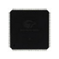
CY7C09579V-100AXC Cypress Semiconductor Corp, CY7C09579V-100AXC Datasheet - Page 3

CY7C09579V-100AXC
Manufacturer Part Number
CY7C09579V-100AXC
Description
IC,SYNC SRAM,32KX36,CMOS,QFP,144PIN,PLASTIC
Manufacturer
Cypress Semiconductor Corp
Specifications of CY7C09579V-100AXC
Format - Memory
RAM
Memory Type
SRAM - Dual Port, Synchronous
Memory Size
1.152M (32K x 36)
Speed
100MHz
Interface
Parallel
Voltage - Supply
3 V ~ 3.6 V
Operating Temperature
0°C ~ 70°C
Package / Case
144-LQFP
Density
1.125Mb
Access Time (max)
12.5ns
Sync/async
Synchronous
Architecture
SDR
Clock Freq (max)
67MHz
Operating Supply Voltage (typ)
3.3V
Address Bus
15b
Package Type
TQFP
Operating Temp Range
0C to 70C
Number Of Ports
2
Supply Current
385mA
Operating Supply Voltage (min)
3.135V
Operating Supply Voltage (max)
3.465V
Operating Temperature Classification
Commercial
Mounting
Surface Mount
Pin Count
144
Word Size
36b
Number Of Words
32K
Lead Free Status / RoHS Status
Contains lead / RoHS non-compliant
Lead Free Status / RoHS Status
Contains lead / RoHS non-compliant
Available stocks
Company
Part Number
Manufacturer
Quantity
Price
Company:
Part Number:
CY7C09579V-100AXC
Manufacturer:
Cypress Semiconductor Corp
Quantity:
10 000
Contents
Pin Configurations ........................................................... 4
Selection Guide ................................................................ 6
Pin Definitions .................................................................. 6
Maximum Ratings ............................................................. 7
Operating Range ............................................................... 7
Electrical Characteristics ................................................. 7
Capacitance ...................................................................... 7
AC Test Load and Waveforms ......................................... 8
Switching Characteristics ................................................ 9
Switching Waveforms .................................................... 11
Flow-Through Output (FT/PIPE = VIL) ............................. 11
Pipelined Operation (FT/PIPE = VIH) ............................... 11
Flow-Through Output (FT/PIPE = VIL) ............................. 12
for Pipelined Operation (FT/PIPE = VIH) .......................... 12
Flow-Through Right Port Read ......................................... 13
(OE Controlled) ................................................................. 15
(OE = VIL) ......................................................................... 16
(OE = VIL) ......................................................................... 17
(OE Controlled) ................................................................. 17
(OE = VIL) ......................................................................... 18
Document Number: 38-06054 Rev. *D
Read Cycle for
Read Cycle for
Bus Match Read Cycle for
Bus Match Read Cycle
Bank Select Pipelined Read ...................................... 13
Left Port Write to
Pipelined Read-to-Write-to-Read (OE = VIL) ............ 14
Pipelined Read-to-Write-to-Read
Bus Match Pipelined Read-to-Write-to-Read
Flow-Through Read-to-Write-to-Read
Flow-Through Read-to-Write-to-Read
Bus Match Flow-Through Read-to-Write-to-Read
Address Counter Advance ................................................ 19
(Flow-Through or Pipelined Outputs) ............................... 20
Address Counter ............................................................... 23
Read/Write and Enable Operation ................................. 24
Address Counter Control Operation ............................. 24
Right Port Configuration ................................................ 25
Right Port Operation ...................................................... 25
Readout of Internal Address Counter ........................... 25
Left Port Operation ......................................................... 25
Counter Operation .......................................................... 26
Bus Match Operation ..................................................... 26
Ordering Information ...................................................... 28
Package Diagrams .......................................................... 29
Sales, Solutions, and Legal Information ...................... 32
Pipelined Read with Address Counter Advance ........ 19
Flow-Through Read with
Write with Address Counter Advance
Counter Reset (Pipelined Outputs) ........................... 21
Counter Reset (Flow-Through Outputs) .................... 22
Pipelined Read of State of Address Counter ............. 23
Flow-Through Read of State of
Long-Word (36-bit) Operation ................................... 26
Word (18-bit) Operation ............................................. 27
Byte (9-bit) Operation ................................................ 27
16K × 36 3.3 V Synchronous Dual-Port SRAM ......... 28
32K × 36 3.3 V Synchronous Dual-Port SRAM ......... 28
Ordering Code Definitions ......................................... 28
Worldwide Sales and Design Support ....................... 32
Products .................................................................... 32
PSoC Solutions ......................................................... 32
CY7C09569V
CY7C09579V
Page 3 of 32
[+] Feedback


