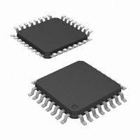
CY7B9950AXC Cypress Semiconductor Corp, CY7B9950AXC Datasheet

CY7B9950AXC
Specifications of CY7B9950AXC
CY7B9950AXC
Available stocks
Related parts for CY7B9950AXC
CY7B9950AXC Summary of contents
Page 1
... Logic Block Diagram REF FB 1F1:0 2F1:0 3F1:0 4F1:0 Cypress Semiconductor Corporation Document #: 38-07338 Rev. *F 2.5 / 3.3 V, 200 MHz High Speed Multi-Phase PLL Clock Buffer Description The CY7B9950 RoboClock eight-output, 200 MHz clock driver. It features output phase programmability which is necessary to optimize the clock tree design of high performance computer and communication systems ...
Page 2
Contents Pinouts .............................................................................. 3 Device Configuration ....................................................... 4 Governing Agencies ......................................................... 4 Absolute Maximum Conditions ....................................... 5 Operating Conditions ....................................................... 5 DC Electrical Specifications at 2.5 V .............................. 5 DC Electrical Specifications at 3.3 V .............................. 6 AC Test Loads ...
Page 3
Pinouts Figure 1. Pin Diagram - 32-Pin TQFP (Top View) Table 1. Pin Definitions [1] Pin Name I/O Type 29 REF I LVTTL/LVCMOS Reference clock input LVTTL 27 TEST I Three-level 22 sOE Two-level 4 ...
Page 4
Device Configuration The outputs of the CY7B9950 can be configured to run at frequencies ranging from 6 to 200 MHz. Banks 3 and 4 output dividers are controlled by 3F[1:0] and 4F[1:0] as indicated in Table 2 and Table 3, ...
Page 5
Absolute Maximum Conditions Parameter Description V Supply voltage DD V Input voltage IN(MIN) V Input voltage IN(MAX) T Temperature, storage S T Temperature, junction J Ø Dissipation, junction to case JC Ø Dissipation, junction to ambient JA ESD ESD protection ...
Page 6
DC Electrical Specifications at 3.3 V Parameter Description V Input LOW voltage IL V Input HIGH voltage IH [9] V Input HIGH voltage IHH [9] V Input MID voltage IMM [9] V Input LOW voltage ILL I Input leakage current ...
Page 7
VTH =1.5V 0.8V 0V 3.3V LVTTL INPUT TEST WAVEFORM AC Input Specifications Parameter Description T ,T Input rise/fall time Input clock pulse PWC T Input duty cycle DCIN F Reference input REF ...
Page 8
Switching Characteristics Parameter Description t Output low time Measured at 0.8 V for V PWL deviation from 50 Output rise/fall time Measured at 0.8 V – 2.0 V for 0.7 V–1.7 V for V ...
Page 9
... Ordering Information Part Number Pb-free ® RoboClock CY7B9950AXC 32 TQFP ® RoboClock CY7B9950AXCT 32 TQFP – Tape and Reel ® RoboClock CY7B9950AXI 32 TQFP ® RoboClock CY7B9950AXIT 32 TQFP – Tape and Reel Ordering Code Definitions CY 7B xxxx A X C/I T Package Drawing Figure 6. 32-Pin Thin Plastic Quad Flatpack 1.0 mm 9.00± ...
Page 10
Acronyms Table 10. Acronyms Used in this Document Acronym Description CLKOUT Clock output CMOS Complementary metal oxide semiconductor DPM Die pick map EPROM Erasable programmable read only memory NTSC National television system committee OE Output enable PAL Phase alternate line ...
Page 11
Document History Page ® Document Title: RoboClock CY7B9950 2.5 / 3.3 V, 200 MHz High Speed Multi-Phase PLL Clock Buffer Document Number: 38-07338 Submission Rev. ECN No. Date ** 121663 11/25/02 *A 122548 12/12/02 *B 124646 03/05/03 *C 433662 See ...
Page 12
... Cypress against all charges. Any Source Code (software and/or firmware) is owned by Cypress Semiconductor Corporation (Cypress) and is protected by and subject to worldwide patent protection (United States and foreign), United States copyright laws and international treaty provisions. Cypress hereby grants to licensee a personal, non-exclusive, non-transferable license to copy, use, modify, create derivative works of, and compile the Cypress Source Code and derivative works for the sole purpose of creating custom software and or firmware in support of licensee product to be used only in conjunction with a Cypress integrated circuit as specified in the applicable agreement ...


