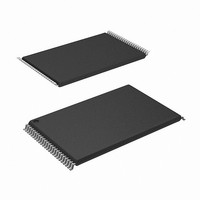
CY62157EV30LL-45ZXAT Cypress Semiconductor Corp, CY62157EV30LL-45ZXAT Datasheet - Page 7

CY62157EV30LL-45ZXAT
Manufacturer Part Number
CY62157EV30LL-45ZXAT
Description
CY62157EV30LL-45ZXAT
Manufacturer
Cypress Semiconductor Corp
Datasheet
1.CY62157EV30LL-45ZSXI.pdf
(17 pages)
Specifications of CY62157EV30LL-45ZXAT
Format - Memory
RAM
Memory Type
SRAM
Memory Size
8M (512K x 16)
Speed
45ns
Interface
Parallel
Voltage - Supply
2.2 V ~ 3.6 V
Operating Temperature
-40°C ~ 85°C
Package / Case
48-TSOP I
Lead Free Status / RoHS Status
Lead free / RoHS Compliant
Switching Characteristics
Over the Operating Range
Notes
Document #: 38-05445 Rev. *H
Read Cycle
t
t
t
t
t
t
t
t
t
t
t
t
t
t
Write Cycle
t
t
t
t
t
t
t
t
t
t
t
14. Test conditions for all parameters other than tri-state parameters assume signal transition time of 3 ns or less, timing reference levels of V
15. AC timing parameters are subject to byte enable signals (BHE or BLE) not switching when chip is disabled. See application note
16. At any temperature and voltage condition, t
17. t
18. If both byte enables are toggled together, this value is 10 ns.
19. The internal write time of the memory is defined by the overlap of WE, CE = V
RC
AA
OHA
ACE
DOE
LZOE
HZOE
LZCE
HZCE
PU
PD
DBE
LZBE
HZBE
WC
SCE
AW
HA
SA
PWE
BW
SD
HD
HZWE
LZWE
levels of 0 to V
write and any of these signals can terminate a write by going inactive. The data input setup and hold timing must be referenced to the edge of the signal that
terminates the write.
HZOE
Parameter
, t
HZCE
[19]
, t
HZBE
CC(typ)
, and t
, and output loading of the specified I
Read cycle time
Address to data valid
Data hold from address change
CE
OE LOW to data valid
OE LOW to LOW-Z
OE HIGH to High-Z
CE
CE
CE
CE
BLE/BHE LOW to data valid
BLE/BHE LOW to Low-Z
BLE/BHE HIGH to HIGH-Z
Write cycle time
CE
Address setup to write end
Address hold from write end
Address setup to write start
WE pulse width
BLE/BHE LOW to write end
Data setup to write end
Data hold from write end
WE LOW to High-Z
WE HIGH to Low-Z
HZWE
1
1
1
1
1
1
[14, 15]
HIGH and CE
LOW and CE
LOW and CE
LOW and CE
HIGH and CE
LOW and CE
transitions are measured when the outputs enter a high-impedance state.
Description
HZCE
2
2
2
2
2
is less than t
2
LOW to High-Z
[16, 17]
[16]
[16]
[16, 17]
HIGH to data valid
HIGH to Low-Z
HIGH to power up
HIGH to write end
LOW to power down
[16, 18]
OL
[16, 17]
/I
LZCE
OH
as shown in the
, t
HZBE
[16, 17]
[16]
is less than t
IL
, BHE, BLE or both = V
45 ns (Ind’l/Auto-A)
AC Test Loads and Waveforms on page
Min
45
10
10
45
35
35
35
35
25
10
LZBE
5
0
5
0
0
0
, t
HZOE
is less than t
Max
45
45
22
18
18
45
45
18
18
IL
, and CE
LZOE
2
, and t
= V
CY62157EV30 MoBL
IH
Min
55
10
10
55
40
40
40
40
25
10
10
55 ns (Auto-E)
5
0
0
0
0
HZWE
. All signals must be active to initiate a
5.
is less than t
AN13842
Max
for further clarification.
55
55
25
20
20
55
55
20
20
CC(typ)
LZWE
for any device.
/2, input pulse
Page 7 of 17
Unit
ns
ns
ns
ns
ns
ns
ns
ns
ns
ns
ns
ns
ns
ns
ns
ns
ns
ns
ns
ns
ns
ns
ns
ns
ns
®
[+] Feedback


