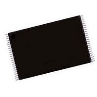
AM29DL800BT-120EC Spansion Inc., AM29DL800BT-120EC Datasheet - Page 22

AM29DL800BT-120EC
Manufacturer Part Number
AM29DL800BT-120EC
Description
Flash Memory IC
Manufacturer
Spansion Inc.
Datasheet
1.AM29DL800BT-70EC.pdf
(46 pages)
Specifications of AM29DL800BT-120EC
Memory Size
8Mbit
Memory Configuration
1M X 8 / 512K X 16
Ic Interface Type
Parallel
Access Time
120ns
Memory Case Style
TSOP
No. Of Pins
48
Operating Temperature Range
0°C To +70°C
Termination Type
SMD
Available stocks
Company
Part Number
Manufacturer
Quantity
Price
Company:
Part Number:
AM29DL800BT-120EC
Manufacturer:
SPANSION
Quantity:
697
Part Number:
AM29DL800BT-120EC
Manufacturer:
AMD
Quantity:
20 000
WRITE OPERATION STATUS
The device provides several bits to determine the sta-
tus of a write operation in the bank where a program or
erase operation is in progress: DQ2, DQ3, DQ5, DQ6,
DQ7, and RY/BY#. Table 6 and the following subsec-
tions describe the function of these bits. DQ7, RY/BY#,
and DQ6 each offer a method for determining whether
a program or erase operation is complete or in
progress. These three bits are discussed first.
DQ7: Data# Polling
The Data# Polling bit, DQ7, indicates to the host sys-
tem w hethe r an Embedded Program or Erase
algorithm is in progress or completed, or whether a
bank is in Erase Suspend. Data# Polling is valid after
the rising edge of the final WE# pulse in the command
sequence.
During the Embedded Program algorithm, the device
outputs on DQ7 the complement of the datum pro-
grammed to DQ7. This DQ7 status also applies to
programming during Erase Suspend. When the Em-
bedded Program algorithm is complete, the device
outputs the datum programmed to DQ7. The system
must provide the program address to read valid status
information on DQ7. If a program address falls within a
protected sector, Data# Polling on DQ7 is active for ap-
proximately 1 µs, then that bank returns to reading
array data.
During the Embedded Erase algorithm, Data# Polling
produces a “0” on DQ7. When the Embedded Erase al-
gorithm is complete, or if the bank enters the Erase
Suspend mode, Data# Polling produces a “1” on DQ7.
The system must provide an address within any of the
sectors selected for erasure to read valid status infor-
mation on DQ7.
After an erase command sequence is written, if all sec-
tors selected for erasing are protected, Data# Polling
on DQ7 is active for approximately 100 µs, then the
bank returns to reading array data. If not all selected
sectors are protected, the Embedded Erase algorithm
erases the unprotected sectors, and ignores the se-
lected sectors that are protected. However, if the
system reads DQ7 at an address within a protected
sector, the status may not be valid.
Just prior to the completion of an Embedded Program
or Erase operation, DQ7 may change asynchronously
with DQ0–DQ6 while Output Enable (OE#) is asserted
low. That is, the device may change from providing sta-
tus information to valid data on DQ7. Depending on
when the system samples the DQ7 output, it may read
the status or valid data. Even if the device has com-
pleted the program or erase operation and DQ7 has
valid data, the data outputs on DQ0–DQ6 may be still
21
Am29DL800B
invalid. Valid data on DQ0–DQ7 will appear on succes-
sive read cycles.
Table 6 shows the outputs for Data# Polling on DQ7.
Figure 5 shows the Data# Polling algorithm. Figure 20
in the AC Characteristics section shows the Data# Poll-
ing timing diagram.
Notes:
1. VA = Valid address for programming. During a sector
2. DQ7 should be rechecked even if DQ5 = “1” because
erase operation, a valid address is any sector address
within the sector being erased. During chip erase, a valid
address is any non-protected sector address.
DQ7 may change simultaneously with DQ5.
No
Figure 5. Data# Polling Algorithm
Read DQ7–DQ0
Read DQ7–DQ0
DQ7 = Data?
DQ7 = Data?
Addr = VA
Addr = VA
DQ5 = 1?
START
FAIL
No
Yes
No
Yes
Yes
PASS


