ADXRS300ABG-REEL Analog Devices Inc, ADXRS300ABG-REEL Datasheet - Page 7
ADXRS300ABG-REEL
Manufacturer Part Number
ADXRS300ABG-REEL
Description
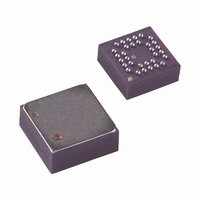
IC,Acceleration Detector,BIPOLAR/MOS,BGA,32PIN,PLASTIC
Manufacturer
Analog Devices Inc
Datasheet
1.ADXRS300EB.pdf
(8 pages)
Specifications of ADXRS300ABG-REEL
Rohs Status
RoHS non-compliant
Range °/s
±300°/s
Sensitivity
5mV/°/s
Typical Bandwidth
40Hz
Voltage - Supply
4.75 V ~ 5.25 V
Current - Supply
6mA
Output Type
Ratiometric
Operating Temperature
-40°C ~ 85°C
Package / Case
32-CSPBGA
For Use With
ADXRS300EB - BOARD EVAL FOR ADXRS300
Lead Free Status / RoHS Status


SETTING BANDWIDTH
External capacitors CMID and C
with on-chip resistors to create two low-pass filters to limit the
bandwidth of the ADXRS300’s rate response. The –3 dB
frequency set by R
and can be well controlled since R
manufacturing to be 180 kΩ ± 1%. Any external resistor applied
between the RATEOUT (1B, 2A) and SUMJ (1C, 2C) pins
results in
The –3 dB frequency is set by RSEN (the parallel combination
of R
controlled since R
sensitivity during manufacturing and have a ±35% tolerance. Its
primary purpose is to limit the high frequency demodulation
artifacts from saturating the final amplifier stage. Thus, this pole
of nominally 400 Hz @ 0.1 µF need not be precise. Lower
frequency is preferable, but its variability usually requires it to
be about 10 times greater (in order to preserve phase integrity)
than the well-controlled output pole. In general, both –3 dB
filter frequencies should be set as low as possible to reduce the
amplitude of these high frequency artifacts and to reduce the
overall system noise.
INCREASING MEASUREMENT RANGE
The full-scale measurement range of the ADXRS300 can be
increased by placing an external resistor between the RATEOUT
(1B, 2A) and SUMJ (1C, 2C) pins, which would parallel the
internal R
example, a 330 kΩ external resistor will give ~50% increase in
the full-scale range. This is effective for up to a 4× increase in
the full-scale range (minimum value of the parallel resistor
allowed is 45 kΩ). Beyond this amount of external sensitivity
reduction, the internal circuitry headroom requirements
prevent further increase in the linear full-scale output range.
The drawbacks of modifying the full-scale range are the
additional output null drift (as much as 2°/sec over temperature)
and the readjustment of the initial null bias (see the Null Adjust
section).
USING THE ADXRS300 WITH A SUPPLY-
RATIOMETRIC ADC
The ADXRS300’s RATEOUT signal is nonratiometric, i.e.,
neither the null voltage nor the rate sensitivity is proportional to
the supply. Rather they are nominally constant for dc supply
changes within the 4.75 V to 5.25 V operating range. If the
ADXRS300 is used with a supply-ratiometric ADC, the
ADXRS300’s 2.5 V output can be converted and used to make
corrections in software for the supply variations.
SEN1
R
f
OUT
OUT
and R
OUT
=
=
(
1
resistor that is factory-trimmed to 180 kΩ. For
180
SEN2
/
(
2
) at about 3.5 kΩ nominal; CMID is less well
×
kΩ
SEN1
OUT
π
×
×
and C
and R
R
R
EXT
OUT
OUT
SEN2
) (
×
/
C
180
is
have been used to trim the rate
OUT
OUT
OUT
kΩ
)
are used in combination
has been trimmed during
×
R
EXT
)
Rev. B | Page 7 of 8
NULL ADJUST
Null adjustment is possible by injecting a suitable current to
SUMJ (1C, 2C). Adding a suitable resistor to either ground or to
the positive supply is a simple way of achieving this. The
nominal 2.5 V null is for a symmetrical swing range at
RATEOUT (1B, 2A). However, a nonsymmetric output swing
may be suitable in some applications. Note that if a resistor is
connected to the positive supply, then supply disturbances may
reflect some null instabilities. Digital supply noise should be
avoided, particularly in this case (see the Supply and Common
Considerations section).
The resistor value to use is approximately
V
null value. If the initial value is below the desired value, the
resistor should terminate on common or ground. If it is above
the desired value, the resistor should terminate on the 5 V
supply. Values are typically in the 1 MΩ to 5 MΩ range.
If an external resistor is used across RATEOUT and SUMJ, then
the parallel equivalent value is substituted into the preceding
equation. Note that the resistor value is an estimate since it
assumes V
SELF-TEST FUNCTION
The ADXRS300 includes a self-test feature that actuates each of
the sensing structures and associated electronics in the same
manner as if subjected to angular rate. It is activated by standard
logic high levels applied to inputs ST1 (5F, 5G), ST2 (4F, 4G), or
both. ST1 causes a voltage at RATEOUT equivalent to typically
–270 mV, and ST2 causes an opposite +270 mV change. The
self-test response follows the viscosity temperature dependence
of the package atmosphere, approximately 0.25%/°C.
Activating both ST1 and ST2 simultaneously is not damaging.
Since ST1 and ST2 are not necessarily closely matched,
actuating both simultaneously may result in an apparent null
bias shift.
CONTINUOUS SELF-TEST
The one-chip integration of the ADXRS300 gives it higher
reliability than is obtainable with any other high volume
manufacturing method. Also, it is manufactured under a mature
BIMOS process that has field-proven reliability. As an additional
failure detection measure, power-on self-test can be performed.
However, some applications may warrant continuous self-test
while sensing rate. Application notes outlining continuous self-
test techniques are also available on the Analog Devices website.
NULL0
R
is the unadjusted zero rate output, and V
NULL
CC
=
= 5.0 V and V
2 (
.
5
×
180
,
000
SUMJ
)
/
(
V
= 2.5 V.
NULL0
–
V
NULL1
ADXRS300
NULL1
)
is the target
Related parts for ADXRS300ABG-REEL
Image
Part Number
Description
Manufacturer
Datasheet
Request
R

Part Number:
Description:
±1.7g Dual-Axis IMEMS Accelerometer Evaluation Board
Manufacturer:
Analog Devices Inc
Datasheet:

Part Number:
Description:
Inertial Sensor Evaluation System
Manufacturer:
Analog Devices Inc
Datasheet:
Part Number:
Description:
Manufacturer:
Analog Devices Inc
Datasheet:
Part Number:
Description:
Manufacturer:
Analog Devices Inc
Datasheet:
Part Number:
Description:
Manufacturer:
Analog Devices Inc
Datasheet:
Part Number:
Description:
Manufacturer:
Analog Devices Inc
Datasheet:
Part Number:
Description:
Manufacturer:
Analog Devices Inc
Datasheet:
Part Number:
Description:
Manufacturer:
Analog Devices Inc
Datasheet:
Part Number:
Description:
Manufacturer:
Analog Devices Inc
Datasheet:
Part Number:
Description:
Manufacturer:
Analog Devices Inc
Datasheet:
Part Number:
Description:
Manufacturer:
Analog Devices Inc
Datasheet:
Part Number:
Description:
Manufacturer:
Analog Devices Inc
Datasheet:
Part Number:
Description:
Manufacturer:
Analog Devices Inc
Datasheet: