ADV202BBCZ-150 Analog Devices Inc, ADV202BBCZ-150 Datasheet
ADV202BBCZ-150
Specifications of ADV202BBCZ-150
Available stocks


Related parts for ADV202BBCZ-150


ADV202BBCZ-150 Summary of contents
Page 1
FEATURES Complete single-chip JPEG2000 compression and decompression solution for video and still images Patented SURF® (spatial ultra-efficient recursive filtering) technology enables low power and low cost wavelet- based compression Supports both 9/7 and 5/3 wavelet transforms with ...
Page 2
ADV202 TABLE OF CONTENTS Features .............................................................................................. 1 Applications....................................................................................... 1 General Description ......................................................................... 1 Functional Block Diagram .............................................................. 1 Revision History ............................................................................... 3 General Description ......................................................................... 4 JPEG2000 Feature Support.......................................................... 4 Specifications..................................................................................... 5 Supply Voltages and Current ...................................................... 5 Input/Output Specifications........................................................ ...
Page 3
REVISION HISTORY 11/06—Rev Rev. C Deleted ANC FIFO References ........................................ Universal Changes to Features ..........................................................................1 Changes to Figure 1...........................................................................1 Changes to JPEG2000 Feature Support Section............................4 Changes to Figure 8.........................................................................10 Changes to Figure 10 ......................................................................11 Changes to Figure 12 ...
Page 4
ADV202 GENERAL DESCRIPTION (continued from Page 1) The ADV202 can process images at a rate of 40 MSPS in reversible mode and at higher rates when used in irreversible mode. The ADV202 contains a dedicated wavelet transform engine, three entropy ...
Page 5
SPECIFICATIONS SUPPLY VOLTAGES AND CURRENT Table 1. Parameter Description VDD DC Supply Voltage, Core IOVDD DC Supply Voltage, I/O PLLVDD DC Supply Voltage, PLL V Input Range INPUT Temp Operating Ambient Temperature Range in Free Air 1 I Static Current ...
Page 6
ADV202 CLOCK AND RESET SPECIFICATIONS Table 3. Parameter Description 1 t MCLK Period MCLK t MCLK Width Low MCLKL t MCLK Width High MCLKH t VCLK Period VCLK t VCLK Width Low VCLKL t VCLK Width High VCLKH t RESET ...
Page 7
NORMAL HOST MODE—READ OPERATION Table 4. Parameter Description t [dir ACK, Direct Registers and FIFO Accesses ACK t [indir ACK, Indirect Registers ACK t [dir] Read Access Time, Direct Registers DRD t [indir] Read Access Time, ...
Page 8
ADV202 NORMAL HOST MODE—WRITE OPERATION Table 5. Parameter Description t (Direct ACK, Direct Registers and FIFO Accesses ACK t (Indirect ACK, Indirect Registers ACK t Data Setup SD t Data Hold HD t Address Setup SA ...
Page 9
DREQ/DACK DMA MODE—SINGLE FIFO WRITE OPERATION Table 6. Parameter Description 1 DREQ DREQ Pulse Width PULSE t DACK Assert to Subsequent DREQ Delay DREQ DACK Setup Data to DACK Deassert Setup SU t Data ...
Page 10
ADV202 DREQ DREQ DACK t WESU WEFB HDATA Figure 7. Fly-By DMA Mode—Single Write Cycle ( DREQ Pulse Width Is Programmable) FSC0 WE FIFO NOT FULL FSRQ0 HDATA PULSE t DREQ DACK HI DACK ...
Page 11
DREQ / DACK DMA MODE—SINGLE FIFO READ OPERATION Table 7. Parameter Description 1 DREQ DREQ Pulse Width PULSE t DACK Assert to Subsequent DREQ Delay DREQ DACK Setup DACK to Data Valid RD t ...
Page 12
ADV202 DREQ DREQ DACK t RDSU RDFB HDATA FCS0 RD FIFO NOT EMPTY FSRQ0 HDATA PULSE t DREQ DACK HI DACK Figure 11. Fly-By DMA Mode—Single Read Cycle ( DREQ Pulse Width Is ...
Page 13
EXTERNAL DMA MODE—FIFO WRITE, BURST MODE Table 8. Parameter Description 1 DREQ DREQ Pulse Width PULSE DREQ Deassert (DR × Pulse = 0) DREQ RTN t DACK to WE Setup DACK SU t Data Setup SU t ...
Page 14
ADV202 DREQ DACK WEFB HDATA EXTERNAL DMA MODE—FIFO READ, BURST MODE Table 9. Parameter Description 1 DREQ DREQ Pulse Width PULSE DREQ Deassert (DR × PULS = 0) DREQ RTN t DACK to RD Setup DACK SU ...
Page 15
DREQ t DREQRTN DACK t DACKSU HDATA t RD Figure 17. Burst Read Cycle for DREQ / DACK DMA Mode for Assigned DMA Channel (EMOD0/EDMOD1[14:11] Programmed to a Value of 0000) t DREQRTN DREQ DACK t ...
Page 16
ADV202 STREAMING MODE (JDATA)—FIFO READ/WRITE Table 10. Parameter Description JDATA MCLK to JDATA Valid TD VALID MCLK to VALID Assert/Deassert TD HOLD HOLD Setup to Rising MCLK SU HOLD HOLD Hold from Rising MCLK HD JDATA JDATA Setup to Rising ...
Page 17
VDATA MODE TIMING Table 11. Parameter Description VDATA VCLK to VDATA Valid Delay (VDATA Output) TD VDATA VDATA Setup to Rising VCLK (VDATA Input) SU VDATA VDATA Hold from Rising VCLK (VDATA Input) HD HSYNC HSYNC Setup to Rising VCLK ...
Page 18
ADV202 RAW PIXEL MODE TIMING Table 12. Parameter Description VDATA VCLK to PIXELDATA Valid Delay (PIXELDATA Output) TD VDATA PIXELDATA Setup to Rising VCLK (PIXELDATA Input) SU VDATA PIXELDATA Hold from Rising VCLK (PIXELDATA Input) HD VRDY VCLK to VRDY ...
Page 19
ABSOLUTE MAXIMUM RATINGS Table 13. Parameter Rating VDD (Supply Voltage, Core) −0 +1.65 V −0 +IOVDD + 0.3 V IOVDD (Supply Voltage, I/O) −0 +1.65 V PLLVDD (Supply Voltage, PLL) Storage Temperature (T ) ...
Page 20
ADV202 PIN BGA ASSIGNMENTS AND FUNCTION DESCRIPTIONS PIN BGA ASSIGNMENTS Table 15. Pin BGA Assignments for 121-Lead Package Pin. No. Pin Location Pin Description 1 A1 DGND 2 A2 HDATA[ VDD 4 A4 DGND 5 A5 HDATA[0] 6 ...
Page 21
Pin. No. Pin Location Pin Description 98 J10 TEST3 99 J11 DGND 100 K1 SCOMM[4] 101 K2 SCOMM[3] 102 K3 SCOMM[0] 103 K4 SCOMM[1] 104 K5 IOVDD 105 K6 IOVDD 106 K7 IOVDD 107 K8 ADDR[2] 108 K9 TEST2 109 ...
Page 22
ADV202 Pin No. Pin Location Pin Description 75 G3 HDATA[20 HDATA[19]_VDATA[15 DGND 78 G6 DGND 79 G7 DGND 80 G8 DGND 81 G9 DGND 82 G10 IRQ 83 G11 ACK 84 G12 HDATA[26]_JDATA[2] ...
Page 23
PIN FUNCTION DESCRIPTIONS Table 17. Pins Used Mnemonic 121-Lead Package MCLK 1 L9 RESET 1 L7 HDATA[15: D1 C3, B5, B4, C2 B1, A2 ADDR[3:0] 4 H11, K8, H10, J9 ...
Page 24
ADV202 Pins Mnemonic Used 121-Lead Package HOLD FCS0 DREQ1 1 F10 FSRQ1 CFG[2] DACK1 1 G9 FCS1 HDATA[31:28 J4, H1 JDATA[7:4] HDATA[27:24 H4, G4 JDATA[3:0] HDATA[23:16] 8 G3, G2, F4, F3, F2 E2, E3, ...
Page 25
Pins Mnemonic Used 121-Lead Package FIELD 1 E10 VSTRB TEST1 1 J6 TEST2 1 K9 TEST3 1 J10 TEST4 1 L6 TEST5 1 K10 VDD A3, A8, D7, H7 DGND A1, A11, A4, A9, C1, C11, D6, E1 ...
Page 26
ADV202 THEORY OF OPERATION The input video or pixel data is passed on to the ADV202’s pixel interface, where samples are de-interleaved and passed on to the wavelet engine, which decomposes each tile or frame into subbands using the 5/3 ...
Page 27
ADV202 INTERFACE There are several possible modes to interface to the ADV202 using the VDATA bus and the HDATA bus or the HDATA bus alone. VIDEO INTERFACE (VDATA BUS) The video interface can be used in applications in which uncompressed ...
Page 28
ADV202 PIN CONFIGURATION AND BUS SIZES/MODES The ADV202 provides a wide variety of control and data configurations, which allows used in many applications with little or no glue logic. The following modes are configured using the BUSMODE ...
Page 29
INTERNAL REGISTERS This section describes the internal registers of the ADV202. DIRECT REGISTERS The ADV202 has 16 direct registers, as listed in Table 19. The direct registers are accessed over the ADDR[3:0], HDATA[31:0 and ...
Page 30
ADV202 INDIRECT REGISTERS In certain modes, such as custom-specific input format or HIPI mode, indirect registers must be accessed by the user through the use of the IADDR and IDATA registers. The indirect register address space starts at Internal Address ...
Page 31
PLL The ADV202 uses the PLL_HI and PLL_LO direct registers to configure the PLL. Any time the PLL_LO register is modified, the host must wait at least 20 μs before reading or writing to any other register. If this delay ...
Page 32
ADV202 VIDEO INPUT FORMATS The ADV202 supports a wide variety of formats for uncompressed video and still image data. The actual interface and bus modes selected for transferring uncompressed data dictates the allowed size of the input data and the ...
Page 33
Table 25. Maximum Supported Tile Width for Data Input on HDATA and VDATA Buses Compression Mode 9/7i 9/7i 9/7i 5/3i 5/3i 5/3i 5/3r 5/3r 5/3r Input Format Tile/Precinct Maximum Width Single-component 2048 Two-component 1024 each Three-component 1024 (Y) Single-component 4096 ...
Page 34
ADV202 APPLICATIONS This section describes typical video applications for the ADV202 JPEG2000 video processor. ENCODE—MULTICHIP MODE Due to the data input rate limitation (see Table 24), an 1080i application requires at least two ADV202s to encode or decode full-resolution 1080i ...
Page 35
DECODE—MULTICHIP MASTER/SLAVE In a master/slave configuration expected that the master HVF outputs are connected to the slave HVF inputs and that each SCOMM[5] pin is connected to the same GPIO on the host. 32-BIT HOST CPU DATA[31:0] ADDR[3:0] ...
Page 36
ADV202 ENCODE/DECODE SDTV VIDEO APPLICATION Figure 27 shows two ADV202 chips using 10-bit CCIR656 in normal host mode. ENCODE MODE 32-BIT HOST CPU DATA[31:0] ADDR[3:0] DECODE MODE 32-BIT HOST CPU DATA[31:0] ADDR[3:0] ADV202 VDATA[11:2] VCLK MCLK HDATA[31:0] INTR IRQ ADDR[3:0] ...
Page 37
ASIC APPLICATION (32-BIT HOST/32-BIT ASIC) Figure 28 shows two ADV202 chips using 10-bit CCIR656 in normal host mode. ASIC DREQ0 DACK0 DATA[31:0] 32-BIT HOST CPU DATA[31:0] ADDR[3:0] ASIC DREQ0 DACK0 DATA[31:0] 31 -BIT HOST CPU DATA[31:0] ADDR[3:0] ADV202 DREQ0 DACK0 ...
Page 38
ADV202 HIPI (HOST INTERFACE—PIXEL INTERFACE) Figure typical configuration using HIPI mode. 32-BIT HOST JDATA INTERFACE Figure 30 shows a typical configuration using JDATA with a dedicated JDATA output, 16-bit host, and 10-bit CCIR656. ASIC 16-BIT HOST CPU ...
Page 39
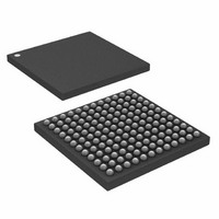
OUTLINE DIMENSIONS DETAIL A * 1.85 1.71 1.40 * 1.85 MAX 12.20 12. 11.80 BALL A1 INDICATOR 10.00 BSC SQ TOP VIEW 1.00 BSC BOTTOM VIEW DETAILA 0.50 NOM 0.30 MIN 0.70 0.60 ...
Page 40
... ADV202BBC-135 −40°C to +85°C 1 ADV202BBCZ-135 −40°C to +85°C ADV202BBC-150 −40°C to +85°C 1 ADV202BBCZ-150 −40°C to +85°C 1 ADV202BBCZRL-150 −40°C to +85°C ADV202-HD-EB ADV202-ASD-P160- Pb-free part. ©2006 Analog Devices, Inc. All rights reserved. Trademarks and registered trademarks are the property of their respective owners ...