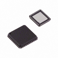
ADUC7020BCPZ62I-RL Analog Devices Inc, ADUC7020BCPZ62I-RL Datasheet - Page 26

ADUC7020BCPZ62I-RL
Manufacturer Part Number
ADUC7020BCPZ62I-RL
Description
IC,MICROCONTROLLER,16-BIT,ARM7 CPU,CMOS,LLCC,40PIN,PLASTIC
Manufacturer
Analog Devices Inc
Series
MicroConverter® ADuC7xxxr
Datasheet
1.USB-I2CLIN-CONV-Z.pdf
(96 pages)
Specifications of ADUC7020BCPZ62I-RL
Core Processor
ARM7
Core Size
16/32-Bit
Speed
44MHz
Connectivity
EBI/EMI, I²C, SPI, UART/USART
Peripherals
PLA, PWM, PSM, Temp Sensor, WDT
Number Of I /o
14
Program Memory Size
62KB (62K x 8)
Program Memory Type
FLASH
Ram Size
8K x 8
Voltage - Supply (vcc/vdd)
2.7 V ~ 3.6 V
Data Converters
A/D 5x12b; D/A 4x12b
Oscillator Type
Internal
Operating Temperature
-40°C ~ 125°C
Package / Case
40-LFCSP
Lead Free Status / RoHS Status
Lead free / RoHS Compliant
For Use With
EVAL-ADUC7020QSZ - KIT DEV ADUC7020 QUICK STARTEVAL-ADUC7020MKZ - KIT MINI DEV FOR ADUC7026/7027
Eeprom Size
-
Lead Free Status / RoHS Status
Lead free / RoHS Compliant
Available stocks
Company
Part Number
Manufacturer
Quantity
Price
Part Number:
ADUC7020BCPZ62I-RL
Manufacturer:
ADI/亚德诺
Quantity:
20 000
ADuC7019/20/21/22/24/25/26/27/28/29
Pin No.
46
47
48
49
50
51
52
53
54
55
56
57
58
59
60
61
62
63
64
65
66
67
68
69
70
71, 72
73, 74
75
76
77
78
79
80
Mnemonic
P3.6/AD6/PWM
P3.7/AD7/PWM
P2.7/PWM1
P2.1/WS/PWM0
P2.2/RS/PWM0
P1.7/SPM7/PLAO[0]
P1.6/SPM6/PLAI[6]
IOGND
IOV
P4.0/AD8/PLAO[8]
P4.1/AD9/PLAO[9]
P1.5/SPM5/PLAI[5]/IRQ3
P1.4/SPM4/PLAI[4]/IRQ2
P1.3/SPM3/PLAI[3]
P1.2/SPM2/PLAI[2]
P1.1/SPM1/PLAI[1]
P1.0/T1/SPM0/PLAI[0]
P4.2/AD10/PLAO[10]
P4.3/AD11/PLAO[11]
P4.4/AD12/PLAO[12]
P4.5/AD13/PLAO[13]
REFGND
V
DAC
DACGND
AGND
AV
DACV
ADC11
ADC0
ADC1
ADC2/CMP0
ADC3/CMP1
REF
DD
DD
REF
DD
L
/MS3
L
TRIP
SYNC
H
/PLAO[7]
/PLAO[6]
/PLAI[14]
/PLAI[15]
General-Purpose Input and Output Port 3.6/External Memory Interface/PWM Safety Cutoff/
Programmable Logic Array Input Element 14.
General-Purpose Input and Output Port 3.7/External Memory Interface/PWM Synchronization/
Programmable Logic Array Input Element 15.
General-Purpose Input and Output Port 2.7/PWM Phase 1 Low-Side Output/External Memory
Select 3.
General-Purpose Input and Output Port 2.1/External Memory Write Strobe/PWM Phase 0 High-
Side Output/Programmable Logic Array Output Element 6.
General-Purpose Input and Output Port 2.2/External Memory Read Strobe/PWM Phase 0 Low-
Side Output/Programmable Logic Array Output Element 7.
Serial Port Multiplexed. General-Purpose Input and Output Port 1.7/UART, SPI/Programmable Logic
Array Output Element 0.
Serial Port Multiplexed. General-Purpose Input and Output Port 1.6/UART, SPI/Programmable Logic
Array Input Element 6.
Ground for GPIO (see Table 78). Typically connected to DGND.
3.3 V Supply for GPIO (see Table 78) and Input of the On-Chip Voltage Regulator.
General-Purpose Input and Output Port 4.0/External Memory Interface/Programmable Logic
Array Output Element 8.
General-Purpose Input and Output Port 4.1/External Memory Interface/Programmable Logic
Array Output Element 9.
Serial Port Multiplexed. General-Purpose Input and Output Port 1.5/UART, SPI/Programmable Logic
Array Input Element 5/External Interrupt Request 3, Active High.
Serial Port Multiplexed. General-Purpose Input and Output Port 1.4/UART, SPI/Programmable Logic
Array Input Element 4/External Interrupt Request 2, Active High.
Serial Port Multiplexed. General-Purpose Input and Output Port 1.3/UART, I2C1/Programmable
Logic Array Input Element 3.
Serial Port Multiplexed. General-Purpose Input and Output Port 1.2/UART, I2C1/Programmable
Logic Array Input Element 2.
Serial Port Multiplexed. General-Purpose Input and Output Port 1.1/UART, I2C0/Programmable
Logic Array Input Element 1.
Serial Port Multiplexed. General-Purpose Input and Output Port 1.0/Timer1 Input/UART, I2C0/
Programmable Logic Array Input Element 0.
General-Purpose Input and Output Port 4.2/External Memory Interface/Programmable Logic
Array Output Element 10.
General-Purpose Input and Output Port 4.3/External Memory Interface/Programmable Logic
Array Output Element 11.
General-Purpose Input and Output Port 4.4/External Memory Interface/Programmable Logic
Array Output Element 12.
General-Purpose Input and Output Port 4.5/External Memory Interface/Programmable Logic
Array Output Element 13.
Ground for the Reference. Typically connected to AGND.
2.5 V Internal Voltage Reference. Must be connected to a 0.47 μF capacitor when using the
internal reference.
External Voltage Reference for the DACs. Range: DACGND to DACV
Analog Ground. Ground reference point for the analog circuitry.
3.3 V Analog Power.
3.3 V Power Supply for the DACs. Must be connected to AV
Single-Ended or Differential Analog Input 11.
Single-Ended or Differential Analog Input 0.
Single-Ended or Differential Analog Input 1.
Single-Ended or Differential Analog Input 2/Comparator Positive Input.
Single-Ended or Differential Analog Input 3/Comparator Negative Input.
Description
Ground for the DAC. Typically connected to AGND.
Rev. C | Page 26 of 96
DD
.
DD
.


