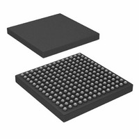
ADSP-21065LKCAZ240 Analog Devices Inc, ADSP-21065LKCAZ240 Datasheet - Page 32

ADSP-21065LKCAZ240
Manufacturer Part Number
ADSP-21065LKCAZ240
Description
ADSP-21065 60 Mhz Mini BGA
Manufacturer
Analog Devices Inc
Series
SHARC®r
Type
Fixed/Floating Pointr
Datasheet
1.ADSP-21065LKSZ-240.pdf
(44 pages)
Specifications of ADSP-21065LKCAZ240
Interface
Host Interface, Serial Port
Clock Rate
60MHz
Non-volatile Memory
External
On-chip Ram
64kB
Voltage - I/o
3.30V
Voltage - Core
3.30V
Operating Temperature
0°C ~ 85°C
Mounting Type
Surface Mount
Package / Case
196-CSPBGA
Lead Free Status / RoHS Status
Lead free / RoHS Compliant
Available stocks
Company
Part Number
Manufacturer
Quantity
Price
Company:
Part Number:
ADSP-21065LKCAZ240
Manufacturer:
Analog Devices Inc
Quantity:
10 000
ADSP-21065L
Serial Ports
Parameter
External Clock
Timing Requirements:
t
t
t
t
t
t
Internal Clock
Timing Requirements:
t
t
t
t
External or Internal Clock
Switching Characteristics:
t
t
External Clock
Switching Characteristics:
t
t
t
t
Internal Clock
Switching Characteristics:
t
t
t
t
t
Enable and Three-State
Switching Characteristics:
t
t
t
t
t
t
External Late Frame Sync
t
t
t
t
NOTES
To determine whether communication is possible between two devices at clock speed n, the following specifications must be confirmed: 1) frame sync delay and frame
sync setup-and-hold, 2) data delay and data setup-and-hold, and 3) SCLK width.
1
2
3
4
*Word selected timing for I
Referenced to sample edge.
SFSE
HFSE
SDRE
HDRE
SCLKW
SCLK
SFSI
HFSI
SDRI
HDRI
DFSE
HOFSE
DFSE
HOFSE
DDTE
HDTE
DFSI
HOFSI
DDTI
HDTI
SCLKIW
DTENE
DDTTE
DTENI
DDTTI
DCLK
DPTR
DDTLFSE
DTENLFSE
DDTLSCK
DTENLSCK
Referenced to drive edge.
MCE = 1, TFS enable and TFS valid follow t
If external RFS/TFS setup to RCLK/TCLK > t
TFS/RFS Setup Before TCLK/RCLK
TFS/RFS Hold After TCLK/RCLK
Receive Data Setup Before RCLK
Receive Data Hold After RCLK
TCLK/RCLK Width
TCLK/RCLK Period
TFS Setup Before TCLK
TFS/RFS Hold After TCLK/RCLK
Receive Data Setup Before RCLK
Receive Data Hold After RCLK
RFS Delay After RCLK (Internally Generated RFS)
RFS Hold After RCLK (Internally Generated RFS)
TFS Delay After TCLK (Internally Generated TFS)
TFS Hold After TCLK (Internally Generated TFS)
Transmit Data Delay After TCLK
Transmit Data Hold After TCLK
TFS Delay After TCLK (Internally Generated TFS)
TFS Hold After TCLK (Internally Generated TFS)
Transmit Data Delay After TCLK
Transmit Data Hold After TCLK
TCLK/RCLK Width
Data Enable from External TCLK
Data Disable from External RCLK
Data Enable from Internal TCLK
Data Disable from Internal TCLK
TCLK/RCLK Delay from CLKIN
SPORT Disable After CLKIN
Data Delay from Late External TFS or External RFS
with MCE = 1, MFD = 0
Data Enable from late FS or MCE = 1, MFD = 0
Data Delay from TCLK/RCLK for Late External
TFS or External RFS with MCE = 1, MFD = 0
Data Enable from RCLK/TCLK for Late External FS or
MCE = 1, MFD = 0
2
S mode is the same as TFS/RFS timing (normal framing only).
DDTENFS
3, 4
SCLK
/2 then t
2
3, 4
and t
; RFS Setup Before RCLK
DDTLFSE.
DDTLSCK
1
1
2
2
2
1
1
2
2
2
2
2
1
1
and t
1
DTENLSCK
–32–
3, 4
3, 4
apply; otherwise t
2
2
2
2
2
2
1
Min
4.0
4.0
1.5
4.0
9.0
t
8.0
1.0
3.0
3.0
3.0
3.0
4.0
–1.5
0.0
(t
5.0
0.0
3.5
4.5
CK
SCLK
DDTLFSE
/2) – 2.5
and t
DTENLFS
apply.
Max
13.0
13.0
12.5
4.5
7.5
10.0
3.0
18.0 + 6 DT
14.0
10.5
12.0
(t
SCLK
/2) + 2.5
REV. C
Unit
ns
ns
ns
ns
ns
ns
ns
ns
ns
ns
ns
ns
ns
ns
ns
ns
ns
ns
ns
ns
ns
ns
ns
ns
ns
ns
ns
ns
ns
ns
ns


