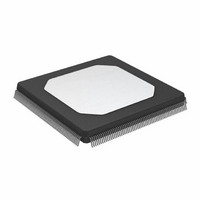
ADSP-21062CSZ-160 Analog Devices Inc, ADSP-21062CSZ-160 Datasheet - Page 24

ADSP-21062CSZ-160
Manufacturer Part Number
ADSP-21062CSZ-160
Description
IC,DSP,32-BIT,CMOS,QFP,240PIN,PLASTIC
Manufacturer
Analog Devices Inc
Series
SHARC®r
Type
Floating Pointr
Specifications of ADSP-21062CSZ-160
Interface
Host Interface, Link Port, Serial Port
Clock Rate
40MHz
Non-volatile Memory
External
On-chip Ram
256kB
Voltage - I/o
5.00V
Voltage - Core
5.00V
Operating Temperature
-40°C ~ 100°C
Mounting Type
Surface Mount
Package / Case
240-MQFP, 240-PQFP
Device Core Size
32b
Architecture
Super Harvard
Format
Floating Point
Clock Freq (max)
40MHz
Mips
40
Device Input Clock Speed
40MHz
Ram Size
256KB
Program Memory Size
Not RequiredKB
Operating Supply Voltage (typ)
5V
Operating Supply Voltage (min)
4.75V
Operating Supply Voltage (max)
5.25V
Operating Temp Range
-40C to 100C
Operating Temperature Classification
Industrial
Mounting
Surface Mount
Pin Count
240
Package Type
MQFP
Package
240MQFP
Numeric And Arithmetic Format
Floating-Point
Maximum Speed
40 MHz
Device Million Instructions Per Second
40 MIPS
Lead Free Status / RoHS Status
Lead free / RoHS Compliant
Lead Free Status / RoHS Status
Lead free / RoHS Compliant
Available stocks
Company
Part Number
Manufacturer
Quantity
Price
Company:
Part Number:
ADSP-21062CSZ-160
Manufacturer:
AD
Quantity:
13 888
Company:
Part Number:
ADSP-21062CSZ-160
Manufacturer:
ADI20
Quantity:
93
Company:
Part Number:
ADSP-21062CSZ-160
Manufacturer:
Analog Devices Inc
Quantity:
10 000
ADSP-21060/ADSP-21060L/ADSP-21062/ADSP-21062L/ADSP-21060C/ADSP-21060LC
Flags
Table 13. Flags
1
Parameter
Timing Requirements
t
t
t
t
Switching Characteristics
t
t
t
t
Flag inputs meeting these setup and hold times for instruction cycle N will affect conditional instructions in instruction cycle N+2.
SFI
HFI
DWRFI
HFIWR
DFO
HFO
DFOE
DFOD
FLAG3–0 OUT
FLAG3–0 IN
RD/WR
CLKIN
CLKIN
FLAG3–0 IN Setup Before CLKIN High
FLAG3–0 IN Hold After CLKIN High
FLAG3–0 IN Delay After RD/WR Low
FLAG3–0 IN Hold After RD/WR Deasserted
FLAG3–0 OUT Delay After CLKIN High
FLAG3–0 OUT Hold After CLKIN High
CLKIN High to FLAG3–0 OUT Enable
CLKIN High to FLAG3–0 OUT Disable
t
DWRFI
t
DFOE
FLAG INPUT
t
SFI
Rev. F | Page 24 of 64 | March 2008
1
t
1
DFO
1
Figure 13. Flags
t
t
HFI
HFIWR
1
FLAG OUTPUT
t
HFO
t
DFO
Min
8 + 5DT/16
0 – 5DT/16
0
4
3
5 V and 3.3 V
t
DFOD
Max
5 + 7DT/16
16
14
Unit
ns
ns
ns
ns
ns
ns
ns
ns


