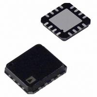
ADP1653ACPZ-R7 Analog Devices Inc, ADP1653ACPZ-R7 Datasheet

ADP1653ACPZ-R7
Specifications of ADP1653ACPZ-R7
Available stocks
Related parts for ADP1653ACPZ-R7
ADP1653ACPZ-R7 Summary of contents
Page 1
FEATURES Small 6.4 mm × 7.2 mm solution 2.2 μH power inductor 92% peak efficiency Tx masking within 50 μs 2 power switch Pin-selectable interface: 2-bit logic or I Programmable flash and torch current Up to 200 ...
Page 2
ADP1653 TABLE OF CONTENTS Features .............................................................................................. 1 Applications....................................................................................... 1 General Description ......................................................................... 1 Typical Operating Circuit................................................................ 1 PCB Layout........................................................................................ 1 Revision History ............................................................................... 2 Specifications..................................................................................... Timing Specifications............................................................ 5 Absolute Maximum Ratings............................................................ 6 Thermal Resistance ...................................................................... 6 ...
Page 3
SPECIFICATIONS −40°C to +125°C, unless otherwise noted Table 1. Parameter SUPPLY 2 Input Voltage Range Undervoltage Lockout Threshold Shutdown Current Soft Power-Down Current 3 Operating Current LX Leakage HPLED ...
Page 4
ADP1653 Parameter HPLED 6 Regulation Voltage Regulation Current INTF = 1, Torch Mode Flash Mode INTF = 0, Flash Mode Torch Mode Step Size for HPLED LSB Change Maximum Flash Timeout SETF RESPONSE (TRANSMIT MASKING FUNCTION) 1 All limits at ...
Page 5
I C TIMING SPECIFICATIONS Table 2. Parameter Min f SCL t 0.6 HIGH t 1.3 LOW t 100 SU, DAT HD, DAT T t 0.6 SU, STA t 0.6 HD, STA t 1.3 BUF t 0.6 ...
Page 6
ADP1653 ABSOLUTE MAXIMUM RATINGS Table 3. Parameter V , CTRL0/SDA, CTRL1/SCL, INTF, EN, DD SETI, SETT, SETF, STR, HPLED to GND INT, ILED to GND LX, OUT to GND PGND to GND Operating Ambient Temperature Range Operating Junction Temperature Storage ...
Page 7
PIN CONFIGURATION AND FUNCTION DESCRIPTIONS Table 5. Pin Function Descriptions Pin No. Mnemonic Description 1 SETT Set Torch Input (2-Bit Logic Interface Only). SETT programs the high power LED current in torch mode. An external resistor connected between SETT and ...
Page 8
ADP1653 Table 6. Mode Selection Pin Mnemonic Value INTF = 0 (I CTRL0/SDA SDA CTRL1/SCL SCL EN Low ADP1653 disabled High ADP1653 enabled STR Low Flash disabled High Flash enabled INT Low Fault condition High Normal operation 1 SETI Resistor ...
Page 9
TYPICAL PERFORMANCE CHARACTERISTICS Δ: 138µ D2812C-2R0 40µs/DIV CHANNEL 0.5A/DIV CHANNEL CHANNEL 0.2A/DIV CHANNEL 4 (STR) 5V/DIV HPLED Figure 5. Startup, Two LEDs Flash Mode, LED ...
Page 10
ADP1653 500 450 400 350 300 250 200 150 100 HPLED CODE Figure 11. HPLED Current vs. HPLED Code 4. ...
Page 11
CHANNEL 0.5A/DIV CHANNEL 3 (INT) 5V/DIV L CHANNEL 0.2A/DIV CHANNEL 4 (STR) 5V/DIV HPLED Figure 17. Flash Untimed Mode, Two LEDs, Timer = 300 ms 380 mA, ...
Page 12
ADP1653 127.5 127.0 126.5 126.0 3V 125.5 125.0 3.6V 124.5 124.0 123.5 123.0 122.5 –40 10 TEMPERATURE (°C) Figure 23. HPLED Regulation, Set at 125 mA, HPLED Register = 00110 (Binary), SETF = V 5.5V 60 110 DD Rev. B ...
Page 13
THEORY OF OPERATION The ADP1653 is a high power, white LED driver ideal for driving white LEDs for use as a camera flash. The ADP1653 includes a step-up converter and a current regulator suitable for powering one ...
Page 14
ADP1653 2-BIT LOGIC INTERFACE MODE (INTF = 1) In 2-bit logic interface mode, the two control pins, CTRL1 and CTRL0, select whether the part is disabled or operating in indicator LED mode, torch mode, or flash mode, as outlined in ...
Page 15
OUT_SEL OUTPUT SELECT CONFIG CONFIGURATION SW_STROBE SOFTWARE STROBE FAULT CONDITIONS The LED regulation current levels are controlled by writing to the ILED and HPLED registers. If the ILED register is set to 0, the ILED regulator is turned off and ...
Page 16
ADP1653 mode, users select flash operation by programming the HPLED register between 12 (01100 binary) and 31 (11111 binary). The flash does not turn on until a strobe command is given by either pulling the STR ...
Page 17
APPLICATIONS INFORMATION FLASH CURRENT FOLDBACK DURING TRANSMIT PULSE The ADP1653 allows a fast, 1.8 V logic-enabled foldback of the flash current, typically enabled shortly before an RF transmit pulse. This feature extends the life of the battery by preventing overstress ...
Page 18
ADP1653 EXTERNAL COMPONENT SELECTION Selecting the Inductor The ADP1653 step-up converter increases the battery voltage to allow driving one, two, or three LEDs, whose combined voltage drop is higher than the battery voltage plus the 0.32 V (typical) current source ...
Page 19
Table 11. Recommended Schottky Diodes PEAK AVE R Vendor (A) (A) (V) Part No BAT20J Rohm RB161VA-20 ON Semi MBR120LSFT1 Philips PMEG2020EJ Selecting the ...
Page 20
ADP1653 PCB LAYOUT Good PCB layout is important to maximize efficiency and to minimize noise and electromagnetic interference (EMI). An example PCB layout is shown in Figure 34. Refer to the following guidelines for adjustments to the suggested layout. The ...
Page 21
SETT 1 OPTIONAL Tx MASK SETF 2 ADP1653 CTRL1/SCL 3 CTRL0/SDA Figure 35. Typical Applications Circuit (High Current Lines Are Shown in Bold) Rev Page INPUT ...
Page 22
... ADP1653 OUTLINE DIMENSIONS PIN 1 INDICATOR 12° MAX 0.90 0.85 0.80 SEATING PLANE ORDERING GUIDE Model Temperature Range ADP1653ACPZ-R7 1 −40°C to +125°C 1 ADP1653-EVALZ RoHS Compliant Part. 3.00 0.60 MAX BSC SQ 0. 2.75 TOP BSC SQ VIEW 9 (BOTTOM VIEW) 0.50 8 BSC 1.50 REF ...
Page 23
NOTES Rev Page ADP1653 ...
Page 24
ADP1653 NOTES ©2007 Analog Devices, Inc. All rights reserved. Trademarks and registered trademarks are the property of their respective owners. D06180-0-9/07(B) Rev Page ...


