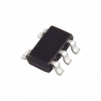
ADP150AUJZ-2.5-R7 Analog Devices Inc, ADP150AUJZ-2.5-R7 Datasheet - Page 13

ADP150AUJZ-2.5-R7
Manufacturer Part Number
ADP150AUJZ-2.5-R7
Description
150mA Ultra-Low Noise LDO
Manufacturer
Analog Devices Inc
Datasheet
1.ADP150-BL1-EVZ.pdf
(20 pages)
Specifications of ADP150AUJZ-2.5-R7
Design Resources
Broadband Low EVM Direct Conversion Transmitter (CN0134) Broadband Low EVM Direct Conversion Transmitter Using LO Divide-by-2 Modulator (CN0144) Using low noise linear drop-out regulators to power wideband PLL & VCO IC's (CN0147)
Regulator Topology
Positive Fixed
Voltage - Output
2.5V
Voltage - Input
Up to 5.5V
Voltage - Dropout (typical)
0.105V @ 150mA
Number Of Regulators
1
Current - Output
150mA (Max)
Current - Limit (min)
190mA
Operating Temperature
-40°C ~ 125°C
Mounting Type
Surface Mount
Package / Case
TSOT-23-5, TSOT-5, TSOP-5
Lead Free Status / RoHS Status
Lead free / RoHS Compliant
Other names
ADP150AUJZ-2.5-R7TR
Available stocks
Company
Part Number
Manufacturer
Quantity
Price
Part Number:
ADP150AUJZ-2.5-R72
Manufacturer:
ADI/亚德诺
Quantity:
20 000
To guarantee the performance of the ADP150, it is imperative
that the effects of the dc bias, temperature, and tolerances on
the behavior of the capacitors be evaluated for each.
UNDERVOLTAGE LOCKOUT
The ADP150 has an internal undervoltage lockout circuit that
disables all inputs and the output when the input voltage is less
than approximately 2.0 V. This ensures that the ADP150 inputs
and output behave in a predictable manner during power-up.
ENABLE FEATURE
The ADP150 uses the EN pin to enable and disable the VOUT
pin under normal operating conditions. As shown in Figure 30,
when a rising voltage on EN crosses the active threshold, V
turns on. When a falling voltage on EN crosses the inactive
threshold, V
As shown in Figure 30, the EN pin has hysteresis built in. This
prevents on/off oscillations that can occur due to noise on the
EN pin as it passes through the threshold points.
The EN pin active/inactive thresholds are derived from the VIN
voltage; therefore, these thresholds vary with changing input
voltage. Figure 31 shows the typical EN active/inactive thresholds
when the input voltage varies from 2.2 V to 5.5 V.
3.5
3.0
2.5
2.0
1.5
1.0
0.5
0
1.1
1.0
0.9
0.8
0.7
0.6
0.5
0.4
Figure 31. Typical EN Pin Thresholds vs. Input Voltage (V
0
2.3
OUT
0.2
turns off.
Figure 30. Typical EN Pin Operation
2.8
0.4
3.3
0.6
3.8
V
V
0.8
EN
IN
FALLING
RISING
(V)
4.3
1.0
4.8
1.2
5.3
1.4
5.5
IN
1.6
)
OUT
Rev. A | Page 13 of 20
The ADP150 uses an internal soft start to limit the inrush current
when the output is enabled. The start-up time for the 3.3 V
option is approximately 150 µs from the time the EN active
threshold is crossed to when the output reaches 90% of its final
value. As shown in Figure 32, the start-up time is dependent on the
output voltage setting.
CURRENT LIMIT AND THERMAL OVERLOAD
PROTECTION
The ADP150 is protected against damage due to excessive
power dissipation by current and thermal overload protection
circuits. The ADP150 is designed to limit current when the
output load reaches 260 mA (typical). When the output load
exceeds 260 mA, the output voltage is reduced to maintain a
constant current limit.
Thermal overload protection is included, which limits the junction
temperature to a maximum of 150°C (typical). Under extreme
conditions (that is, high ambient temperature and power dissipation)
when the junction temperature starts to rise above 150°C, the
output is turned off, reducing the output current to zero. When
the junction temperature drops below 135°C, the output is turned
on again and the output current is restored to its nominal value.
Consider the case where a hard short from VOUT to GND occurs.
At first, the ADP150 limits current so that only 260 mA is
conducted into the short. If self-heating of the junction is great
enough to cause its temperature to rise above 150°C, thermal
shutdown activates, turning off the output and reducing the
output current to zero. As the junction temperature cools and
drops below 135°C, the output turns on and conducts 260 mA
into the short, again causing the junction temperature to rise
above 150°C. This thermal oscillation between 135°C and 150°C
causes a current oscillation between 260 mA and 0 mA that
continues as long as the short remains at the output.
Current and thermal limit protections are intended to protect
the device against accidental overload conditions. For reliable
operation, device power dissipation must be externally limited
so that the junction temperatures do not exceed 125°C.
1
1 1 1
CH1 1V
CH3 1V
Figure 32. Typical Start-Up Time
CH2 1V
CH4 1V
T
M40.0µs
T
240.000ns
V
V
V
A CH1
OUT
OUT
OUT
EN
= 3.3V
= 2.8V
= 1.8V
ADP150
3.24V


