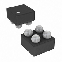
ADP150ACBZ-3.0-R7 Analog Devices Inc, ADP150ACBZ-3.0-R7 Datasheet - Page 17

ADP150ACBZ-3.0-R7
Manufacturer Part Number
ADP150ACBZ-3.0-R7
Description
150mA LDO 3.0Vout
Manufacturer
Analog Devices Inc
Datasheet
1.ADP150-BL1-EVZ.pdf
(20 pages)
Specifications of ADP150ACBZ-3.0-R7
Design Resources
Broadband Low EVM Direct Conversion Transmitter (CN0134) Broadband Low EVM Direct Conversion Transmitter Using LO Divide-by-2 Modulator (CN0144) Using low noise linear drop-out regulators to power wideband PLL & VCO IC's (CN0147)
Regulator Topology
Positive Fixed
Voltage - Output
3V
Voltage - Input
Up to 5.5V
Voltage - Dropout (typical)
0.105V @ 150mA
Number Of Regulators
1
Current - Output
150mA (Max)
Current - Limit (min)
190mA
Operating Temperature
-40°C ~ 125°C
Mounting Type
Surface Mount
Package / Case
4-WLCSP
Lead Free Status / RoHS Status
Lead free / RoHS Compliant
Other names
ADP150ACBZ-3.0-R7TR
ADP150
PCB LAYOUT CONSIDERATIONS
Heat dissipation from the package can be improved by
increasing the amount of copper attached to the pins of the
ADP150. However, as listed in Table 7, a point of diminishing
returns is reached eventually, beyond which an increase in the
copper size does not yield significant heat dissipation benefits.
Place the input capacitor as close as possible to the VIN and
GND pins. Place the output capacitor as close as possible to the
VOUT and GND pins. Use of 0402 size or 0603 size capacitors
and resistors achieves the smallest possible footprint solution on
boards where area is limited.
Figure 48. Example WLCSP PCB Layout
Figure 47. Example TSOT PCB Layout
Rev. A | Page 17 of 20


