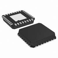
ADN8830ACP Analog Devices Inc, ADN8830ACP Datasheet - Page 2

ADN8830ACP
Manufacturer Part Number
ADN8830ACP
Description
IC,Temperature Sensor Interface,LLCC,32PIN,CERAMIC
Manufacturer
Analog Devices Inc
Datasheet
1.ADN8830ACPZ-REEL7.pdf
(24 pages)
Specifications of ADN8830ACP
Applications
Thermoelectric Cooler
Current - Supply
8mA
Voltage - Supply
3.3 V ~ 5 V
Operating Temperature
-40°C ~ 85°C
Mounting Type
Surface Mount
Package / Case
32-LFCSP
Lead Free Status / RoHS Status
Contains lead / RoHS non-compliant
Other names
ADN8830ACP-WP
ADN8830ACP-WP
ADN8830ACP-WP
Available stocks
Company
Part Number
Manufacturer
Quantity
Price
Company:
Part Number:
ADN8830ACP
Manufacturer:
AD
Quantity:
317
Company:
Part Number:
ADN8830ACPZ
Manufacturer:
ADI
Quantity:
317
Part Number:
ADN8830ACPZ
Manufacturer:
ADI/亚德诺
Quantity:
20 000
ADN8830–SPECIFICATIONS
Parameter
TEMPERATURE STABILITY
PWM OUTPUT DRIVERS
LINEAR OUTPUT AMPLIFIER
POWER SUPPLY
ERROR AMPLIFIER
REFERENCE VOLTAGE
OSCILLATOR
LOGIC CONTROL*
*Logic inputs meet typical CMOS I/O conditions for source/sink current (~1 A).
Specifications subject to change without notice.
Long-Term Stability
Output Transition Time
Nonoverlapping Clock Delay
Output Resistance
Output Voltage Swing
Output Voltage Ripple
Output Current Ripple
Output Resistance
Output Voltage Swing
Power Supply Voltage
Power Supply Rejection Ratio
Supply Current
Shutdown Current
Soft-Start Charging Current
Undervoltage Lockout
Input Offset Voltage
Gain
Input Voltage Range
Common-Mode Rejection Ratio
Open-Loop Input Impedance
Gain-Bandwidth Product
Reference Voltage
Synchronization Range
Oscillator Frequency
Logic Low Input Threshold
Logic High Input Threshold
Logic Low Output Level
Logic High Output Threshold
t
R
OUT A
R
R
OUT B
V
PSRR
I
I
I
V
V
A
V
CMRR
R
GBW
V
f
f
Symbol
CLK
CLK
R
SY
SD
SS
OUT A
I
O
O, P2
O, N2
DD
OLOCK
OS
V, IN
CM
IN
REF
, t
TEC
(N1, P1)
F
Conditions
Using 10 k thermistor with
C
I
V
f
f
I
I
V
–40 C
PWM not switching
–40 C
Pin 10 = 0 V
Low-to-high threshold
V
0.2 V < V
–40 C
I
Pin 25 connected to external clock
Pin 24 = V
Pin 25 = GND)
CLK
CLK
L
OUT
OUT
REF
LIM
DD
CM
L
= –4.4% at 25 C
(@ V
configuration as shown in Figure 1, unless otherwise noted.)
= 50 mA
= 3,300 pF
< 2 mA
= 1 MHz
= 1 MHz
= 3.3 V to 5 V, V
= 1.5 V
= 2 mA
= 2 mA
= 0 V
DD
T
T
T
= 3.3 V to 5.0 V, V
CM
A
A
A
DD
–2–
< 2.0 V
; (R = 150 k ;
+85 C
+85 C
+85 C
TEC
GND
= 0 V
= 0 V, T
A
= 25 C, T
Min
50
0
0
3.0
80
60
0.2
58
55
2.37
800
3
V
200
DD
– 0.2
SET
= 25 C, using typical application
Typ
20
65
6
0.2
0.2
85
178
92
8
5
15
2.0
50
20
68
1
2
2.47
1,000
Max
0.01
V
V
5.5
12
15
2.7
250
2.0
2.57
1,000
1,250
0.2
0.2
DD
DD
REV. C
Unit
ns
ns
V
%
%
V
V
dB
dB
mA
mA
V
V/V
V
dB
dB
G
MHz
V
kHz
kHz
V
V
V
V
C
A
A
V


