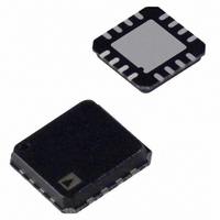
ADN2890ACPZ-RL Analog Devices Inc, ADN2890ACPZ-RL Datasheet

ADN2890ACPZ-RL
Specifications of ADN2890ACPZ-RL
Related parts for ADN2890ACPZ-RL
ADN2890ACPZ-RL Summary of contents
Page 1
FEATURES SFP reference design available Input sensitivity p rise/fall times CML outputs: 700 mV p-p differential Programmable LOS detector signal strength indicator (RSSI): SFF-8472 compliant average power measurement Single-supply operation: ...
Page 2
ADN2890 TABLE OF CONTENTS Specifications..................................................................................... 3 Absolute Maximum Ratings............................................................ 5 Thermal Resistance ...................................................................... 5 ESD Caution.................................................................................. 5 Pin Configuration and Function Descriptions............................. 6 Typical Performance Characteristics ............................................. 7 Theory of Operation ........................................................................ 8 LIMAMP ....................................................................................... 8 REVISION HISTORY Revision 0: ...
Page 3
SPECIFICATIONS VCC = VEE = MIN MAX A MIN Table 1. Parameter QUANTIZER DC CHARACTERISTICS Input Voltage Range Input Common Mode Peak-to-Peak Differential Input Range Input Sensitivity Input Offset Voltage Input ...
Page 4
ADN2890 Parameter LOGIC OUTPUTS (LOS Output High Voltage Output Low Voltage OL Min Typ Max 2.4 0.4 Rev Page Unit Test Conditions/Comments V Open drain output, 4.7 kΩ − 10 ...
Page 5
ABSOLUTE MAXIMUM RATINGS Table 2. Parameter Supply Voltage Minimum Input Voltage (All Inputs) Maximum Input Voltage (All Inputs) Storage Temperature Operating Temperature Range Lead Temperature Range (Soldering 10 s) Junction Temperature ESD CAUTION ESD (electrostatic discharge) sensitive device. Electrostatic charges ...
Page 6
ADN2890 PIN CONFIGURATION AND FUNCTION DESCRIPTIONS Note: There is an exposed pad on the bottom of the package that must be connected to the GND plane with filled vias. Table 4. Pin Function Descriptions Pin No. Mnemonic 1 AVCC 2 ...
Page 7
TYPICAL PERFORMANCE CHARACTERISTICS 0.96 0.88 0.80 0.72 0.64 0.56 0.48 0.40 0.32 0.24 0.16 0. 0.1 0.2 0.3 0.4 0.5 0.6 RSSI_IN (mA) Figure 3. RSSI Output vs. Average PIN Photodiode Current 0.014 0.012 0.010 0.008 0.006 0.004 ...
Page 8
ADN2890 THEORY OF OPERATION LIMAMP Input Buffer The limiting amplifier has differential inputs (PIN/NIN), with an internal 50 Ω termination. The ROSA (receive optical sub- assembly) is typically ac-coupled to the ADN2890 inputs, although dc coupling is possible. An internal ...
Page 9
APPLICATIONS INFORMATION PCB DESIGN GUIDELINES Proper RF PCB design techniques must be used for optimal performance. Power Supply Connections and Ground Planes Use of one low impedance ground plane is recommended. The VEE pins should be soldered directly to the ...
Page 10
ADN2890 PCB Layout Figure 9 shows a recommended PC board layout. Use of 50 Ω transmission lines is required for all high frequency input and output signals to minimize reflections: PIN, NIN, OUTP and OUTN also necessary for ...
Page 11
OUTLINE DIMENSIONS PIN 1 INDICATOR 12° MAX 1.00 0.85 0.80 SEATING PLANE ORDERING GUIDE Model Temperature Range ADN2890ACP –40°C to +85°C ADN2890ACP-RL –40°C to +85°C ADN2890ACP-RL7 –40°C to +85°C 3.00 0.60 MAX BSC SQ 13 0.45 12 2.75 TOP VIEW ...
Page 12
ADN2890 NOTES © 2004 Analog Devices, Inc. All rights reserved. Trademarks and registered trademarks are the property of their respective owners. D04509–0–5/04(0) Rev Page ...


