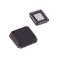
ADN2870ACPZ-RL Analog Devices Inc, ADN2870ACPZ-RL Datasheet

ADN2870ACPZ-RL
Specifications of ADN2870ACPZ-RL
Available stocks
Related parts for ADN2870ACPZ-RL
ADN2870ACPZ-RL Summary of contents
Page 1
FEATURES SFP/SFF MSA and SFF-8472 compliant SFP reference design available 50 Mbps to 3.3 Gbps operation Dual-loop control of average power and extinction ratio Typical rise/fall time 60 ps Bias current range 100 mA Modulation current range ...
Page 2
ADN2870 TABLE OF CONTENTS Features .............................................................................................. 1 Applications ....................................................................................... 1 General Description ......................................................................... 1 Applications Diagram ...................................................................... 1 Revision History ............................................................................... 2 Specifications ..................................................................................... 3 SFP Timing Specifications ............................................................... 5 Absolute Maximum Ratings ............................................................ 6 ESD Caution .................................................................................. 6 Pin ...
Page 3
SPECIFICATIONS 3.6 V. All specifications T CC Table 1. Parameter LASER BIAS CURRENT (IBIAS) Output Current IBIAS Compliance Voltage IBIAS when ALS High CCBIAS Compliance Voltage MODULATION CURRENT (IMODP, IMODN) Output Current IMOD Compliance Voltage ...
Page 4
ADN2870 Parameter SUPPLY (with respect to GND Temperature range: −40°C to +85°C. 2 Measured into a 15 Ω load (22 Ω resistor in parallel with digital scope 50 Ω input) using a 11110000 ...
Page 5
SFP TIMING SPECIFICATIONS Table 2. Parameter ALS Assert Time 1 ALS Negate Time Time to Initialize, Including Reset of FAIL FAIL Assert Time ALS to Reset Time 1 Guaranteed by design and characterization. Not production tested DATAP DATAN ...
Page 6
ADN2870 ABSOLUTE MAXIMUM RATINGS Table 3. Parameter VCC to GND IMODN, IMODP PAVCAP, ERCAP, PAVSET, PAVREF, ERREF, IBIAS, IBMON, IMMON, ALS, CCBIAS, RPAV, ERSET, FAIL DATAP, DATAN (Single-Ended Differential) Junction Temperature Operating Temperature Range Industrial Storage Temperature Range Junction Temperature ...
Page 7
PIN CONFIGURATION AND FUNCTION DESCRIPTIONS Table 4. Pin Function Descriptions Pin No. Mnemonic 1 CCBIAS 2 PAVSET 3 GND 4 VCC 5 PAVREF 6 RPAV 7 ERCAP 8 PAVCAP 9 GND 10 DATAP 11 DATAN 12 ALS 13 ERSET 14 ...
Page 8
ADN2870 TYPICAL PERFORMANCE CHARACTERISTICS MODULATION CURRENT (mA) Figure 6. Rise Time vs. Modulation Current MODULATION CURRENT (mA) Figure 7. Fall Time vs. ...
Page 9
TEMPERATURE (°C) Figure 12. IBIAS/IBMON Gain vs. Temperature, I OC48 PRBS31 DATA TRANSMISSION t LESS THAN 1μs _OFF ALS Figure 13. ALS Assert Time, ...
Page 10
ADN2870 OPTICAL WAVEFORMS V = 3.3 V and T = 25°C, unless otherwise noted. Note that in Figure 18 through Figure 22, there is no change to the PAVCAP and CC A ERCAP values using either of the lasers or ...
Page 11
THEORY OF OPERATION Laser diodes have a current-in to light-out transfer function, as shown in Figure 23. Two key characteristics of this transfer function are the threshold current, Ith, and slope in the linear region beyond the threshold current, referred ...
Page 12
ADN2870 Operation with Lasers with Temperature-Dependent Nonlinearity of Laser LI Curve The ADN2870 ERCL extracts information from the monitor photodiode signal relating to the slope of the LI characteristics at the Optical 1 level (P1). For lasers with good linearity ...
Page 13
Tx_FAULT Tx_FAIL V CC MPD PAVSET ANALOG DEVICES MICROCONTROLLER PAVREF DAC ADC RPAV 1kΩ GND ERREF DAC ERSET 1kΩ GND Figure 26. Using MicroConverter Calibration and Monitoring PAVREF MPD RPAV PAVSET GND ERSET V ...
Page 14
ADN2870 RESISTOR SETPOINT CALIBRATION In resistor setpoint calibration, PAVREF, ERREF, and RPAV pins must all be tied to VCC. Average power and extinction ratio can be set using the PAVSET and ERSET pins, respectively. A resistor is placed between the ...
Page 15
V CC PHOTODIODE PAVSET ADN2870 µC ADC INPUT R Figure 31. Single Measurement of I Sense Resistor in Resistor Setpoint I LOOP BANDWIDTH SELECTION To ensure that the ADN2870 control loops have sufficient bandwidth, the average power loop capacitor (PAVCAP) ...
Page 16
ADN2870 LASER DIODE INTERFACING The schematic in Figure 32 describes the recommended circuit for interfacing the ADN2870 to most TO-Can or coax lasers. These lasers typically have impedances of 5 Ω Ω and have axial leads. The circuit ...
Page 17
ALARMS The ADN2870 has a latched active high monitoring alarm (FAIL). The FAIL alarm output is an open drain in conformance to SFP MSA specification requirements. The ADN2870 has a three-fold alarm system that recognizes: • Use of a bias ...
Page 18
... INDICATOR 1.00 0.85 0.80 SEATING PLANE ORDERING GUIDE Model Temperature Range 1 ADN2870ACPZ −40°C to +85°C 1 ADN2870ACPZ-RL −40°C to +85°C ADN2870ACPZ-RL7 1 −40°C to +85° RoHS Compliant Part. 4.00 BSC SQ 0.60 MAX 0.50 BSC TOP 3.75 VIEW BSC SQ 0.50 0.40 ...
Page 19
NOTES Rev Page ADN2870 ...
Page 20
ADN2870 NOTES ©2004–2008 Analog Devices, Inc. All rights reserved. Trademarks and registered trademarks are the property of their respective owners. D04510-0-3/08(A) Rev Page Error! Unknown document property name. ...


