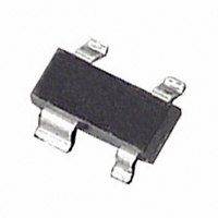
ADM811-3TARTZ-RL7 Analog Devices Inc, ADM811-3TARTZ-RL7 Datasheet - Page 6

ADM811-3TARTZ-RL7
Manufacturer Part Number
ADM811-3TARTZ-RL7
Description
IC,VOLT DETECTOR,FIXED,+3.08V,CMOS,TO-253LOW,4PIN,PLASTIC
Manufacturer
Analog Devices Inc
Type
Simple Reset/Power-On Resetr
Specifications of ADM811-3TARTZ-RL7
Package / Case
SOT-143, SOT-143B, TO-253AA
Mounting Type
Surface Mount
Operating Temperature
-40°C ~ 85°C
Output
Push-Pull, Totem Pole
Reset
Active Low
Number Of Voltages Monitored
1
Reset Timeout
140 ms Minimum
Voltage - Threshold
3.08V
Lead Free Status / RoHS Status
Lead free / RoHS Compliant
Available stocks
Company
Part Number
Manufacturer
Quantity
Price
ADM811/ADM812
CIRCUIT INFORMATION
Reset Thresholds
A reset output is provided to the microprocessor whenever the
V
old is dependent on whether an L, M, T, S, R, or Z suffix is
used. Refer to Table I.
RESET OUTPUT
On power-up and after V
internal timer holds the reset output active for 240 ms (typical).
This is intended as a power-on reset signal for the processor. It
allows time for both the power supply and the microprocessor to
stabilize after power-up. If a power supply brownout or inter-
ruption occurs, the reset output is similarly activated and remains
active for 240 ms (typical) after the supply recovers. This allows
time for the power supply and microprocessor to stabilize.
The ADM811 provides an active low reset output (RESET)
while the ADM812 provides an active high output (RESET).
During power-down of the ADM811, the RESET output remains
valid (low) with V
processor is held in a stable shutdown condition as the supply
falls and also ensures that no spurious activity can occur via
the microprocessor as it powers up.
MANUAL RESET
The ADM811/ADM812 is equipped with a manual reset input.
This input is designed to operate in a noisy environment where
unwanted glitches could be induced. These glitches could be
produced by the bouncing action of a switch contact, or where a
manual reset switch may be located some distance away from
the circuit (the cabling of which may pick-up noise).
The manual reset input is guaranteed to ignore logically valid
inputs that are faster than 100 ns and to accept inputs longer in
duration than 10 µs.
CC
input is below the reset threshold. The actual reset thresh-
Model
ADM811LART
ADM811MART
ADM811TART
ADM811-3TART
ADM811SART
ADM811RART
ADM811ZART
ADM812LART
ADM812MART
ADM812TART
ADM812SART
ADM812RART
ADM812ZART
Table I. Reset Threshold Options
CC
as low as 1 V. This ensures that the micro-
CC
rises above the reset threshold, an
Reset
Threshold (V)
4.63
4.38
3.08
3.08
2.93
2.63
2.32
4.63
4.38
3.08
2.93
2.63
2.32
–6–
Glitch Immunity
The ADM811/ADM812 contains internal filtering circuitry
providing glitch immunity from fast transient glitches on the
power supply line.
INTERFACING TO OTHER DEVICES
Output
The ADM811/ADM812 is designed to integrate with as many
devices as possible. One feature of the ADM811/ADM812 is
the reset output, which is directly proportional to V
guaranteed only while V
part to be used with both 3 V and 5 V, or any nominal voltage
within the minimum and maximum specifications for V
BENEFITS OF A VERY ACCURATE RESET THRESHOLD
Because the ADM811/ADM812 can operate effectively even when
there are large degradations of the supply voltages, the possibility
of a malfunction during a power failure is greatly reduced. Another
advantage of the ADM811/ADM812 is its very accurate internal
voltage reference circuit. Combined, these benefits produce an
exceptionally reliable microprocessor supervisory circuit.
ENSURING A VALID RESET OUTPUT DOWN TO V
When V
no longer sinks current. Therefore, a high impedance CMOS
logic input connected to RESET may drift to undetermined
logic levels. To eliminate this problem, a 100 kΩ resistor should
be connected from RESET to ground.
RESET
Figure 3. Ensuring a Valid RESET Output
Down to V
V
CC
CC
V
t
falls below 0.8 V, the ADM811/ADM812’s RESET
1
REF
= RESET TIME = 240ms TYPICAL
Figure 2. Power Fail RESET Timing
= RESET VOLTAGE THRESHOLD
V
REF
CC
t
= 0 V
1
ADM811
CC
GND
V
V
V
CC
CC
is greater than 1 V). This enables the
REF
RESET
V
REF
t
1
CC
(this is
V
CC
CC
REV. C
REF
.
= 0 V


