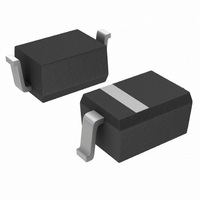
MM3Z2V4T1 SERIES
Zener Voltage Regulators
200 mW SOD−323 Surface Mount
mount package that has a power dissipation of 200 mW. They are
designed to provide voltage regulation protection and are especially
attractive in situations where space is at a premium. They are well
suited for applications such as cellular phones, hand held portables,
and high density PC boards.
Specification Features:
•
•
•
•
•
•
•
Mechanical Characteristics:
CASE:
FINISH:
MAXIMUM CASE TEMPERATURE FOR SOLDERING PURPOSES:
LEADS:
POLARITY:
FLAMMABILITY RATING:
MOUNTING POSITION:
Stresses exceeding Maximum Ratings may damage the device. Maximum
Ratings are stress ratings only. Functional operation above the Recommended
Operating Conditions is not implied. Extended exposure to stresses above the
Recommended Operating Conditions may affect device reliability.
1. FR−4 Minimum Pad
MAXIMUM RATINGS
© Semiconductor Components Industries, LLC, 2006
Total Device Dissipation FR−5 Board,
Thermal Resistance, Junction−to−Ambient
Junction and Storage Temperature Range
This series of Zener diodes is packaged in a SOD−323 surface
260°C for 10 Seconds
0.067” x 0.049” (1.7 mm x 1.25 mm)
Standard Zener Breakdown Voltage Range − 2.4 V to 75 V
Steady State Power Rating of 200 mW
Small Body Outline Dimensions:
Low Body Height: 0.035” (0.9 mm)
Package Weight: 4.507 mg/Unit
ESD Rating of Class 3 (>16 kV) per Human Body Model
Pb−Free Packages are Available
(Note 1) @ T
Derate above 25°C
Void-free, Transfer-Molded Plastic
All External Surfaces are Corrosion Resistant
Plated with Pb−Sn or Sn Only (Pb−Free)
Cathode Indicated by Polarity Band
A
Rating
= 25°C
Any
UL 94 V−0
Symbol
T
R
J
P
, T
qJA
D
stg
−65 to +150
Max
200
635
1.5
1
mW/°C
°C/W
Unit
mW
°C
†For information on tape and reel specifications,
See specific marking information in the device marking
column of the Electrical Characteristics table on page 2 of
this data sheet.
MM3ZxxxT1
MM3ZxxxT1G
including part orientation and tape sizes, please
refer to our Tape and Reel Packaging Specifications
Brochure, BRD8011/D.
Device
(Note: Microdot may be in either location)
*Date Code orientation may vary depending
DEVICE MARKING INFORMATION
upon manufacturing location.
ORDERING INFORMATION
Cathode
xx = Specific Device Code
M = Date Code*
G = Pb−Free Package
MARKING DIAGRAM
1
(Pb−Free)
SOD−323
SOD−323
1
Package
CASE 477
SOD−323
STYLE 1
xx
G
2
G
3000/Tape & Reel
3000/Tape & Reel
Anode
2
Shipping†