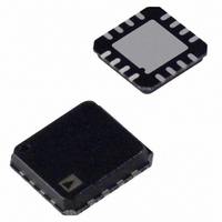
ADL5561ACPZ-R7 Analog Devices Inc, ADL5561ACPZ-R7 Datasheet - Page 15

ADL5561ACPZ-R7
Manufacturer Part Number
ADL5561ACPZ-R7
Description
Low Distortion 3V 41mA Diff Amp
Manufacturer
Analog Devices Inc
Datasheet
1.ADL5561ACPZ-R7.pdf
(24 pages)
Specifications of ADL5561ACPZ-R7
Amplifier Type
RF/IF Differential
Number Of Circuits
1
Output Type
Differential
Slew Rate
9800 V/µs
-3db Bandwidth
2.9GHz
Current - Input Bias
3µA
Current - Supply
40mA
Voltage - Supply, Single/dual (±)
3 V ~ 3.6 V
Operating Temperature
-40°C ~ 85°C
Mounting Type
Surface Mount
Package / Case
16-VFQFN, 16-CSP, Exposed Pad
Voltage - Supply
3 V ~ 3.6 V
Frequency
2.9GHz
Rf Type
General Purpose
Gain
15.5dB
Noise Figure
8dB
P1db
19dBm
Lead Free Status / RoHS Status
Lead free / RoHS Compliant
Test Frequency
-
Lead Free Status / RoHS Status
Lead free / RoHS Compliant
Other names
ADL5561ACPZ-R7TR
Available stocks
Company
Part Number
Manufacturer
Quantity
Price
Company:
Part Number:
ADL5561ACPZ-R7
Manufacturer:
MICREL
Quantity:
1 000
Part Number:
ADL5561ACPZ-R7
Manufacturer:
ADI/亚德诺
Quantity:
20 000
INPUT AND OUTPUT INTERFACING
The ADL5561 can be configured as a differential input to
differential output driver, as shown in Figure 32. The differential
broadband input is provided by the ETC1-1-13 balun transformer,
and the two 34.8 Ω resistors provide a 50 Ω input match for
the three input impedances that change with the variable gain
strapping. The input and output 0.1 μF capacitors isolate the
VCC/2 bias from the source and balanced load. The load must be
200 Ω to provide the expected ac performance (see the Specifications
section and the Typical Performance Characteristics section).
Table 4. Differential Termination Values for Figure 32
Gain (dB)
6
12
15.5
The differential gain of the AD5561 is dependent on the source
impedance and load, as shown in Figure 33.
The differential gain can be determined using the following
formula. The values of R
shown in Table 5.
Table 5. Values of R
Gain (dB)
6
12
15.5
1
1
NOTES
1. FOR 6dB GAIN (A
2. FOR 12dB GAIN (A
3. FOR 15.5dB GAIN (A
AC
50Ω
/
/
2
2
AND INPUT B TO BOTH VIN1 AND VIN2.
R
R
S
S
Figure 32. Differential-Input-to-Differential-Output Configuration
A
V
0.1µF
0.1µF
=
ETC1-1-13
400
R
IN
Figure 33. Differential Input Loading Circuit
×
V
R1
V
10
R2
= 2), CONNECT INPUT A TO VIP1 AND INPUT B TO VIN1.
= 4), CONNECT INPUT A TO VIP2 AND INPUT B TO VIN2.
V
VIP2
VIP1
VIN1
VIN2
R
= 6), CONNECT INPUT A TO BOTH VIP1 AND VIP2
+
0.1µF
0.1µF
L
IN
R
for Differential Gain
L
100Ω
200Ω
200Ω
100Ω
IN
A
B
R1 (Ω)
28.7
33.2
for each gain configuration are
40.2
VIP2
VIP1
VIN1
VIN2
400Ω
400Ω
3.3V
R
200
100
66.7
IN
(Ω)
5Ω
5Ω
0.1µF
0.1µF
R2 (Ω)
28.7
33.2
40.2
0.1µF
0.1µF
R
R
2
2
L
L
R
R
2
2
L
L
Rev. B | Page 15 of 24
(1)
Single-Ended Input to Differential Output
The ADL5561 can also be configured in a single-ended input
to differential output driver, as shown in Figure 34. In this
configuration, the gain of the part is reduced due to the
application of the signal to only one side of the amplifier. The
strappable gain values are listed in Table 6 with the required
terminations to match to a 50 Ω source using R1 and R2. Note
that R1 must equal the parallel value of the source and R2. The
input and output 0.1 μF capacitors isolate the VCC/2 bias from
the source and the balanced load. The performance for this
configuration is shown in Figure 11, Figure 14, and Figure 20.
Table 6. Single-Ended Termination Values for Figure 34
Gain (dB)
5.6
11.1
14.1
The single-ended gain configuration of the ADL5561 is dependent
on the source impedance and load, as shown in Figure 35.
AC
R
S
Figure 34. Single-Ended Input to Differential-Output Configuration
R2
NOTES
1. FOR 5.6dB GAIN (A
2. FOR 11.1dB GAIN (A
3. FOR 14.1dB GAIN (A
AC
50Ω
AND INPUT B TO VIN1.
AND INPUT B TO VIN2.
VIP1 AND VIP2 AND INPUT B TO BOTH VIN1 AND VIN2.
R1
0.1µF
Figure 35. Single-Ended Input Loading Circuit
+
R2
0.1µF
0.1µF
R1
VIP2
VIP1
VIN1
VIN2
+
A
B
V
0.1µF
V
V
= 1.9), CONNECT INPUT A TO VIP1
100Ω
200Ω
200Ω
100Ω
= 3.6), CONNECT INPUT A TO VIP2
= 5.1), CONNECT INPUT A TO BOTH
R1 (Ω)
27
29
30
VIP2
VIP1
VIN1
VIN2
3.3V
400Ω
400Ω
0.1µF
0.1µF
5Ω
5Ω
R2 (Ω)
60
69
77
ADL5561
R
R
2
2
L
L
0.1µF
0.1µF
R
R
2
2
L
L


