ADIS16364BMLZ Analog Devices Inc, ADIS16364BMLZ Datasheet - Page 2
ADIS16364BMLZ
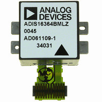
Manufacturer Part Number
ADIS16364BMLZ
Description
Hi-Precision Tri-Axis Inertial Sensor
Manufacturer
Analog Devices Inc
Series
iSensor™r
Datasheet
1.ADIS16364PCBZ.pdf
(20 pages)
Specifications of ADIS16364BMLZ
Output Type
Digital - SPI
Sensor Type
Gyroscope and Accelerometer
No. Of Axes
3
Ic Interface Type
Serial
Sensor Case Style
ML-24-2
No. Of Pins
24
Supply Voltage Range
4.75V To 5.25V
Operating Temperature Range
-40°C To +105°C
Lead Free Status / RoHS Status
Lead free / RoHS Compliant
For Use With
ADIS16364/PCBZ - BOARD EVAL FOR ADIS16364
Lead Free Status / Rohs Status
Compliant
Available stocks
Company
Part Number
Manufacturer
Quantity
Price
Company:

Part Number:
ADIS16364BMLZ
Manufacturer:
ON
Quantity:
93 000


ADIS16364
TABLE OF CONTENTS
Features .............................................................................................. 1
Applications....................................................................................... 1
General Description ......................................................................... 1
Functional Block Diagram .............................................................. 1
Revision History ............................................................................... 2
Specifications..................................................................................... 3
Absolute Maximum Ratings............................................................ 6
Pin Configuration and Function Descriptions............................. 7
Typical Performance Characteristics ............................................. 8
Theory of Operation ........................................................................ 9
REVISION HISTORY
2/11—Rev. C to Rev. D
Changes to Gyroscopes Misalignment and Accelerometers
Misalignment Test Conditions/Comments, Table 1 .................... 3
Changes to Table 30 and Table 31 ................................................ 16
8/10—Rev. B to Rev. C
Reorganized Layout............................................................Universal
Changes to Features Section............................................................ 1
Changes to Table 1............................................................................ 3
Changes to Table 2............................................................................ 5
Changes to Table 5............................................................................ 7
Changes to Table 7, Reading Sensor Data Section,
and Device Configuration Section................................................. 9
Changes to Table 8.......................................................................... 10
Changes to Burst Read Data Collection Section, Output Data
Registers Section, and Table 9....................................................... 11
Added Table 10, Table 11, Table 12, Table 13, and Table 14;
Renumbered Tables Sequentially.................................................. 11
Changes to Internal Sample Rate Section.................................... 12
Added Sensor Bandwidth Section and Figure 14;
Renumbered Figures Sequentially................................................ 13
Changes to Digital Filtering Section and Table 20 ..................... 13
Changes to General-Purpose I/O Section................................... 14
Changes to Table 26........................................................................ 15
Timing Specifications .................................................................. 5
Timing Diagrams.......................................................................... 5
ESD Caution.................................................................................. 6
Basic Operation ............................................................................ 9
Reading Sensor Data.................................................................... 9
Device Configuration .................................................................. 9
Rev. D | Page 2 of 20
Applications Information .............................................................. 17
Outline Dimensions ....................................................................... 18
Changes to Table 29 and Table 31 ................................................ 16
Added Product Identification Section......................................... 16
Added Applications Information Section, Figure 17,
and Figure 18................................................................................... 17
Moved Input ADC Channel Section and Figure 16................... 17
3/09—Rev. A to Rev. B
Changes to Features Section ............................................................1
Changes to Figure 5 and Figure 6....................................................7
Changes to Figure 7...........................................................................8
Changes to Devices Configuration Section ...................................9
Changes to Figure 12...................................................................... 10
Changes to Output Data Registers Section ................................. 11
Changes to Internal Sample Rate Section, Power Management
Section, Digital Filtering Section, and the Dynamic Range
Section.............................................................................................. 12
3/09—Rev. 0 to Rev. A
Changes to Features Section and General Description Section..1
Changes to Table 1.............................................................................3
Changes to Table 9.......................................................................... 11
Changes to Table 20 ....................................................................... 14
1/09—Revision 0: Initial Version
Memory Map .............................................................................. 10
Burst Read Data Collection ...................................................... 11
Output Data Registers ............................................................... 11
Calibration................................................................................... 12
Operational Control................................................................... 12
Input/Output Functions ............................................................ 14
Diagnostics.................................................................................. 15
Product Identification................................................................ 16
Installation/Handling................................................................. 17
Gyroscope Bias Optimization................................................... 17
Input ADC Channel................................................................... 17
Interface Printed Circuit Board (PCB).................................... 17
Ordering Guide .......................................................................... 18
Related parts for ADIS16364BMLZ
Image
Part Number
Description
Manufacturer
Datasheet
Request
R

Part Number:
Description:
±1.7g Dual-Axis IMEMS Accelerometer Evaluation Board
Manufacturer:
Analog Devices Inc
Datasheet:

Part Number:
Description:
Inertial Sensor Evaluation System
Manufacturer:
Analog Devices Inc
Datasheet:
Part Number:
Description:
Manufacturer:
Analog Devices Inc
Datasheet:
Part Number:
Description:
Manufacturer:
Analog Devices Inc
Datasheet:
Part Number:
Description:
Manufacturer:
Analog Devices Inc
Datasheet:
Part Number:
Description:
Manufacturer:
Analog Devices Inc
Datasheet:
Part Number:
Description:
Manufacturer:
Analog Devices Inc
Datasheet:
Part Number:
Description:
Manufacturer:
Analog Devices Inc
Datasheet:
Part Number:
Description:
Manufacturer:
Analog Devices Inc
Datasheet:
Part Number:
Description:
Manufacturer:
Analog Devices Inc
Datasheet:
Part Number:
Description:
Manufacturer:
Analog Devices Inc
Datasheet:
Part Number:
Description:
Manufacturer:
Analog Devices Inc
Datasheet:
Part Number:
Description:
Manufacturer:
Analog Devices Inc
Datasheet: