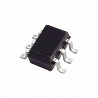
ADG849YKSZ-REEL7 Analog Devices Inc, ADG849YKSZ-REEL7 Datasheet - Page 9

ADG849YKSZ-REEL7
Manufacturer Part Number
ADG849YKSZ-REEL7
Description
IC,ANALOG SWITCH,SINGLE,SPDT,CMOS,TSSOP,6PIN,PLASTIC
Manufacturer
Analog Devices Inc
Type
Analog Switchr
Datasheet
1.ADG849YKSZ-REEL.pdf
(12 pages)
Specifications of ADG849YKSZ-REEL7
Function
Switch
Circuit
1 x SPDT
On-state Resistance
600 mOhm
Voltage Supply Source
Single Supply
Voltage - Supply, Single/dual (±)
5V
Current - Supply
0.001µA
Operating Temperature
-40°C ~ 125°C
Mounting Type
Surface Mount
Package / Case
6-TSSOP, SC-88, SOT-363
Multiplexer Configuration
Single SPDT
Number Of Inputs
1
Number Of Outputs
2
Number Of Channels
1
Analog Switch On Resistance
1.1@3.6VOhm
Analog Switch Turn On Time
22ns
Analog Switch Turn Off Time
18ns
Package Type
SC-70
Power Supply Requirement
Single
Single Supply Voltage (min)
1.8V
Single Supply Voltage (typ)
3/5V
Single Supply Voltage (max)
5.5V
Dual Supply Voltage (min)
Not RequiredV
Dual Supply Voltage (typ)
Not RequiredV
Dual Supply Voltage (max)
Not RequiredV
Power Dissipation
0.00001W
Supply Current
0.001mA
Mounting
Surface Mount
Pin Count
6
Operating Temp Range
-40C to 125C
Operating Temperature Classification
Automotive
Package
6SC-70
Maximum On Resistance
1.1@3.6V Ohm
Maximum High Level Output Current
400 mA
Maximum Turn-off Time
18@3.6V ns
Maximum Turn-on Time
22@3.6V ns
Switch Architecture
SPDT
Power Supply Type
Single
Lead Free Status / RoHS Status
Lead free / RoHS Compliant
Lead Free Status / RoHS Status
Lead free / RoHS Compliant
Available stocks
Company
Part Number
Manufacturer
Quantity
Price
Company:
Part Number:
ADG849YKSZ-REEL7
Manufacturer:
ON
Quantity:
400
Part Number:
ADG849YKSZ-REEL7
Manufacturer:
ADI/亚德诺
Quantity:
20 000
TEST CIRCUITS
V
S
Figure 15. On-Resistance
R
S
ON
= V1/I
I
V1
DS
V
DS
D
S
IN
V
V
S
S
0.1µF
S2
S1
IN
IN
0.1µF
S2
S1
GND
V
V
DD
DD
D
GND
V
V
GND
DD
DD
V
DD
D
S2
S1
D
50Ω
R L
Figure 19. Break-Before-Make Time Delay, t
V
S
50Ω
1nF
R L
Figure 18. Switching Times, t
I
S
35pF
C
NC
V
(OFF)
L
OUT
V
Figure 20. Charge Injection
OUT
Figure 16. Off-Leakage
35pF
C
L
Rev. 0| Page 9 of 12
V
OUT
S
V
V
IN
OUT
SW ON
D
∆V
V
V
IN
OUT
I
D
V
V
OUT
IN
OUT
(OFF)
0V
ON
, t
Q
80%
OFF
INJ
V
D
= CL × ∆V
SW OFF
t
t
50%
BBM
BBM
50%
ON
90%
OUT
80%
NC
50%
50%
t
90%
BBM
t
OFF
Figure 17. On-Leakage
S
D
I
D
(ON)
A
ADG849
V
D


