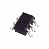
ADG841YKSZ-REEL7 Analog Devices Inc, ADG841YKSZ-REEL7 Datasheet

ADG841YKSZ-REEL7
Specifications of ADG841YKSZ-REEL7
Related parts for ADG841YKSZ-REEL7
ADG841YKSZ-REEL7 Summary of contents
Page 1
FEATURES Ultralow on resistance 0.28 Ω typical 0.48 Ω max at 125°C Excellent audio performance, ultralow distortion 0.025 Ω typical 0.052 Ω max R flatness ON 1. 3.6 V single supply High current carrying capability 300 mA continuous ...
Page 2
ADG841/ADG842 TABLE OF CONTENTS Specifications—2 3.6 V......................................................... 3 Specifications—2.5 V ± 0.2 V.......................................................... 4 Specifications—1. 1.95 ........................................................ 5 Absolute Maximum Ratings............................................................ 6 ESD Caution.................................................................................. 6 Pin Configuration and Function Descriptions............................. 7 REVISION HISTORY 4/05—Revision 0: Initial ...
Page 3
SPECIFICATIONS— 3.6 V, GND = 0 V, unless otherwise noted. DD Table 2. Parameter ANALOG SWITCH Analog Signal Range On Resistance ( Resistance Flatness (R ) FLAT (ON) ...
Page 4
ADG841/ADG842 SPECIFICATIONS—2.5 V ± 0 2.5 V ± 0.2 V, GND = 0 V, unless otherwise noted. DD Table 3. Parameter ANALOG SWITCH Analog Signal Range On Resistance ( Resistance Flatness (R ) FLAT ...
Page 5
SPECIFICATIONS—1. 1. 1.65 V to1.95 V, GND = 0 V, unless otherwise noted. DD Table 4. Parameter ANALOG SWITCH Analog Signal Range On Resistance ( Resistance Flatness (R ) FLAT (ON) LEAKAGE CURRENTS ...
Page 6
ADG841/ADG842 ABSOLUTE MAXIMUM RATINGS T = 25°C, unless otherwise noted. A Table 5. Parameter Rating V to GND −0 +4 Analog Inputs −0 Digital Inputs −0 4 ...
Page 7
PIN CONFIGURATION AND FUNCTION DESCRIPTIONS Table 6. Pin Function Descriptions Pin No. Mnemonic GND ADG841/ ADG842 TOP VIEW (Not ...
Page 8
ADG841/ADG842 TYPICAL PERFORMANCE CHARACTERISTICS 0.350 T = 25° 100mA DS 0.325 0.300 0.275 V = 3.3V DD 0.250 0.225 0.200 0 0.4 0.8 1.2 1.6 2.0 2.4 SOURCE VOLTAGE (V) Figure 3. On ...
Page 9
V = 3.3V DD 150 100 50 0 –50 –100 –40 – TEMPERATURE (°C) Figure 9. Leakage Current vs. Temperature, V 140 V = 2.5V DD 120 100 –20 ...
Page 10
ADG841/ADG842 25° 3.3V/2.5V/1.8V DD –20 –40 –60 –80 –100 –120 100 1k 10k 100k FREQUENCY (Hz) Figure 15. Off Isolation vs. Frequency 0.030 0.025 0.020 V = 1.8V 0.015 ...
Page 11
TERMINOLOGY I DD Positive supply current Analog voltage on Terminals D and Ohmic resistance between D and S. R FLAT (ON) Flatness is the difference between the maximum and minimum value of ...
Page 12
ADG841/ADG842 TEST CIRCUITS Figure 18. On Resistance V DD 0.1 µ 0.1 µ 0.1 µ ...
Page 13
... OUTLINE DIMENSIONS 0.10 MAX ORDERING GUIDE Model Temperature Range 2 ADG841YKSZ-500RL7 –40°C to +125°C 2 ADG841YKSZ-REEL –40°C to +125°C ADG841YKSZ-REEL7 2 –40°C to +125°C 2 ADG842YKSZ-500RL7 –40°C to +125°C ADG842YKSZ-REEL 2 –40°C to +125°C 2 ADG842YKSZ-REEL –40°C to +125°C 1 Branding on this package is limited to three characters due to space constraints. ...
Page 14
ADG841/ADG842 NOTES Rev Page ...
Page 15
NOTES Rev Page ADG841/ADG842 ...
Page 16
ADG841/ADG842 NOTES © 2005 Analog Devices, Inc. All rights reserved. Trademarks and registered trademarks are the property of their respective owners. D05424-0-4/05(0) Rev Page ...


