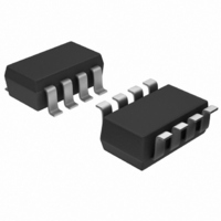
ADG619BRTZ-500RL7 Analog Devices Inc, ADG619BRTZ-500RL7 Datasheet - Page 5

ADG619BRTZ-500RL7
Manufacturer Part Number
ADG619BRTZ-500RL7
Description
IC,ANALOG SWITCH,SINGLE,SPDT,CMOS,TSSOP,8PIN,PLASTIC
Manufacturer
Analog Devices Inc
Datasheet
1.ADG619BRTZ-REEL7.pdf
(16 pages)
Specifications of ADG619BRTZ-500RL7
Function
Switch
Circuit
1 x SPDT
On-state Resistance
6.5 Ohm
Voltage Supply Source
Dual Supply
Voltage - Supply, Single/dual (±)
±2.7 V ~ 5.5 V
Current - Supply
0.0001µA
Operating Temperature
-40°C ~ 85°C
Mounting Type
Surface Mount
Package / Case
SOT-23-8
Lead Free Status / RoHS Status
Lead free / RoHS Compliant
SINGLE SUPPLY
V
Table 3.
Parameter
ANALOG SWITCH
LEAKAGE CURRENTS
DIGITAL INPUTS
DYNAMIC CHARACTERISTICS
POWER REQUIREMENTS
1
2
Temperature range for B version is −40°C to +85°C.
Guaranteed by design, not subject to production test.
DD
Analog Signal Range
On Resistance (R
R
On-Resistance Flatness (R
Source Off Leakage, I
Channel On Leakage, I
Input High Voltage, V
Input Low Voltage, V
Input Current, I
Digital Input Capacitance, C
ADG619
Break-Before-Make Time Delay, t
ADG620
Make-Before-Break Time Delay, t
Charge Injection
Off Isolation
Channel-to-Channel Crosstalk
Bandwidth −3 dB
C
C
I
DD
ON
S
D
= 5 V ± 10%, V
, C
t
t
t
t
(OFF)
ON
OFF
ON
OFF
Match Between Channels (ΔR
S
(ON)
INL
ON
SS
or I
)
= 0 V, GND = 0 V. All specifications −40°C to +85°C, unless otherwise noted.
INL
INH
S
INH
(Off )
D
, I
S
FLAT (ON)
(On)
2
IN
)
BBM
MBB
ON
)
+25°C
7
10
0.8
1.1
0.5
±0.01
±0.25
±0.01
±0.25
0.005
2
120
220
50
75
70
50
85
210
340
170
6
−67
−67
190
25
95
0.001
B Version
Rev. C | Page 5 of 16
−40°C to +85°C
0 V to V
12.5
1.3
0.5
1.2
±1
±1
2.4
0.8
±0.1
280
110
10
110
420
10
1.0
1
DD
Unit
V
Ω typ
Ω max
Ω typ
Ω max
Ω typ
Ω max
nA typ
nA max
nA typ
nA max
V min
V max
μA typ
μA max
pF typ
ns typ
ns max
ns typ
ns max
ns typ
ns min
ns typ
ns max
ns typ
ns max
ns typ
ns min
pC typ
dB typ
dB typ
MHz typ
pF typ
pF typ
μA typ
μA max
Test Conditions/Comments
V
V
V
V
V
V
V
V
R
V
R
V
R
V
R
V
R
V
R
V
V
R
22
R
23
R
f = 1 MHz
f = 1 MHz
V
Digital inputs = 0 V or 5.5 V
S
S
L
L
L
L
L
L
L
L
L
DD
S
S
DD
S
IN
S
S
S1
S
S
S
S
DD
= 50 Ω, C
= 50 Ω, C
= 0 V to 4.5 V, I
= 0 V to 4.5 V, I
= 1.5 V to 3.3 V, I
= 1 V/4.5 V, V
= V
= 300 Ω, C
= 3.3 V; see Figure 18
= 300 Ω, C
= 3.3 V; see Figure 18
= 300 Ω, C
= 300 Ω, C
= 3.3 V; see Figure 18
= 300 Ω, C
= 3.3 V; see Figure 18
= 300 Ω, C
= 3.3 V; see Figure 20
= 0 V, R
= 50 Ω, C
= V
= V
= 4.5 V, V
= 5.5 V
= 5.5 V
D
INL
S2
= 1 V/4.5 V; see Figure 17
= 3.3 V; see Figure 19
or V
S
= 0 Ω, C
L
L
L
= 5 pF, f = 1 MHz; see Figure
= 5 pF, f = 1 MHz; see Figure
SS
INH
L
L
L
L
L
L
= 5 pF; see Figure 24
= 35 pF
= 35 pF
= 35 pF
= 35 pF
= 35 pF
= 35 pF
D
= 0 V
ADG619/ADG620
= 4.5 V/1 V; see Figure 16
DS
DS
= −10 mA; see Figure 15
DS
L
= −10mA
= 1 nF; see Figure 21
= −10 mA


