ADG2188YCPZ-HS-RL7 Analog Devices Inc, ADG2188YCPZ-HS-RL7 Datasheet - Page 17

ADG2188YCPZ-HS-RL7
Manufacturer Part Number
ADG2188YCPZ-HS-RL7
Description
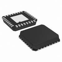
IC,ANALOG SWITCH,SINGLE,8X8 CROSSPOINT,CMOS,LLCC,32PIN,PLASTIC
Manufacturer
Analog Devices Inc
Series
I²Cr
Datasheet
1.ADG2188YCPZ-HS-RL7.pdf
(28 pages)
Specifications of ADG2188YCPZ-HS-RL7
Function
Crosspoint Switch
Circuit
1 x 8:8
On-state Resistance
50 Ohm
Voltage Supply Source
Single Supply
Voltage - Supply, Single/dual (±)
12V, 15V
Current - Supply
.05µA
Operating Temperature
-40°C ~ 125°C
Mounting Type
Surface Mount
Package / Case
32-VFQFN, CSP Exposed Pad
Lead Free Status / RoHS Status
Lead free / RoHS Compliant
For Use With
EVAL-ADG2188EBZ - BOARD EVAL FOR ADG2188
Lead Free Status / RoHS Status
Lead free / RoHS Compliant
Other names
ADG2188YCPZ-HS-RL7TR
Available stocks
Company
Part Number
Manufacturer
Quantity
Price
Company:
Part Number:
ADG2188YCPZ-HS-RL7
Manufacturer:
Maxim
Quantity:
101
TERMINOLOGY
On Resistance (R
The series on-channel resistance measured between the
X input/output and the Y input/output.
On Resistance Match (ΔR
The channel-to-channel matching of on resistance when
channels are operated under identical conditions.
On Resistance Flatness (R
The variation of on resistance over the specified range produced
by the specified analog input voltage change with a constant
load current.
Channel Off Leakage (I
The sum of leakage currents into or out of an off channel input.
Channel On Leakage (I
The current loss/gain through an on-channel resistance,
creating a voltage offset across the device.
Input Leakage Current (I
The current flowing into a digital input when a specified low
level or high level voltage is applied to that input.
Input Off Capacitance (C
The capacitance between an analog input and ground when the
switch channel is off.
Input/Output On Capacitance (C
The capacitance between the inputs or outputs and ground
when the switch channel is on.
Digital Input Capacitance (C
The capacitance between a digital input and ground.
Output On Switching Time (t
The time required for the switch channel to close. The time is
measured from 50% of the logic input change to the time the
output reaches 10% of the final value.
Output Off Switching Time (t
The time required for the switch to open. This time is measured
from 50% of the logic input change to the time the output
reaches 90% of the switch off condition.
ON
)
ON
OFF
)
IN
OFF
ON
FLAT(ON)
)
)
)
)
IN
ON
OFF
)
)
)
)
ON
)
Rev. 0 | Page 17 of 28
Total Harmonic Distortion + Noise (THD + N)
The ratio of the harmonic amplitudes plus noise of a signal to
the fundamental.
−3 dB Bandwidth
The frequency at which the output is attenuated by 3 dB.
Off Isolation
The measure of unwanted signal coupling through an off switch.
Crosstalk
The measure of unwanted signal that is coupled through from
one channel to another as a result of parasitic capacitance.
Differential Gain
The measure of how much color saturation shift occurs when
the luminance level changes. Both attenuation and amplification
can occur; therefore, the largest amplitude change between any
two levels is specified and is expressed as a percentage of the
largest chrominance amplitude.
Differential Phase
The measure of how much hue shift occurs when the luminance
level changes. It can be a negative or positive value and is
expressed in degrees of subcarrier phase.
Charge Injection
The measure of the glitch impulse transferred from the digital
input to the analog output during on/off switching.
Input High Voltage (V
The minimum input voltage for Logic 1.
Input Low Voltage (V
The maximum input voltage for Logic 0.
Output Low Voltage (V
The minimum input voltage for Logic 1.
Input Low Voltage (V
The maximum output voltage for Logic 0.
I
Positive supply current.
I
Negative supply current.
DD
SS
INL
INL
INH
OL
)
)
)
)
ADG2188


